When it comes online in 2030, the High-Luminosity LHC (HL-LHC) will feel like a new collider. The hearts of the ATLAS and CMS detectors, and 1.2 km of the 27 km-long Large Hadron Collider (LHC) ring will have been transplanted with cutting-edge technologies that will push searches for new physics into uncharted territory.
On the accelerator side, one of the most impactful upgrades will be the brand-new final focusing systems just before the proton or ion beams arrive at the interaction points. In the new “inner triplets”, particles will slalom in a more focused and compacted way than ever before towards collisions inside the detectors.
To achieve the required focusing strength, the new quadrupole magnets will use Nb3Sn conductors for the first time in an accelerator. Nb3Sn will allow fields as high as 11.5 T, compared to 8.5 T for the conventional NbTi bending magnets used elsewhere in the LHC. As they are a new technology, an integrated test stand of the full 60 m-long inner-triplet assembly is essential – and work is now in full swing.
Learning opportunity
“The main challenge at this stage is the interconnections between the magnets, particularly the interfaces between the magnets and the cryogenic line,” explains Marta Bajko, who leads work on the inner-triplet-string test facility. “During this process, we have encountered nonconformities, out-of-tolerance components, and other difficulties – expected challenges given that these connections are being made for the first time. This phase is a learning opportunity for everyone involved, allowing us to refine the installation process.”
The last magnet – one of two built in the US – is expected to be installed in May. Before then, the so-called N lines, which enable the electrical connections between the different magnets, will be pulled through the entire magnet chain to prepare for splicing the cables together. Individual system tests and short-circuit tests have already been successfully performed and a novel alignment system developed for the HL-LHC is being installed on each magnet. Mechanical transfer function measurements of some magnets are ongoing, while electrical integrity tests in a helium environment have been successfully completed, along with the pressure and leak test of the superconducting link.
“Training the teams is at the core of our focus, as this setup provides the most comprehensive and realistic mock-up before the installations are to be done in the tunnel,” says Bajko. “The surface installation, located in a closed and easily accessible building near the teams’ workshops and laboratories, offers an invaluable opportunity for them to learn how to perform their tasks effectively. This training often takes place alongside other teams, under real installation constraints, allowing them to gain hands-on experience in a controlled yet authentic environment.”
The inner triplet string is composed of a separation and recombination dipole, a corrector-package assembly and a quadrupole triplet. The dipole combines the two counter-rotating beams into a single channel; the corrector package fine-tunes beam parameters; and the quadrupole triplet focuses the beam onto the interaction point.
Quadrupole triplets have been a staple of accelerator physics since they were first implemented in the early 1950s at synchrotrons such as the Brookhaven Cosmotron and CERN’s Proton Synchrotron. Quadrupole magnets are like lenses that are convex (focusing) in one transverse plane and concave (defocusing) in the other, transporting charged particles like beams of light on an optician’s bench. In a quadrupole triplet, the focusing plane alternates with each quadrupole magnet. The effect is to precisely focus the particle beams onto tight spots within the LHC experiments, maximising the number of particles that interact, and increasing the statistical power available to experimental analyses.
Nb3Sn is strategically important because it lays the foundation for future high-energy colliders
Though quadrupole triplets are a time-honoured technique, Nb3Sn brings new challenges. The HL-LHC magnets are the first accelerator magnets to be built at lengths of up to 7 m, and the technical teams at CERN and in the US collaboration – each of which is responsible for half the total “cold mass” production – have decided to produce two variants, primarily driven by differences in available production and testing infrastructure.
Since 2011, engineers and accelerator physicists have been hard at work designing and testing the new magnets and their associated powering, vacuum, alignment, cryogenic, cooling and protection systems. Each component of the HL-LHC will be individually tested before installation in the LHC tunnel, however, this is only half the story as all components must be integrated and operated within the machine, where they will all share a common electrical and cooling circuit. Throughout the rest of 2025, the inner-triplet string will test the integration of all these components, evaluating them in terms of their collective behaviour, in preparation for hardware commissioning and nominal operation.
“We aim to replicate the operational processes of the inner-triplet string using the same tools planned for the HL-LHC machine,” says Bajko. “The control systems and software packages are in an advanced stage of development, prepared through extensive collaboration across CERN, involving three departments and nine equipment groups. The inner-triplet-string team is coordinating these efforts and testing them as if operating from the control room – launching tests in short-circuit mode and verifying system performance to provide feedback to the technical teams and software developers. The test programme has been integrated into a sequencer, and testing procedures are being approved by the relevant stakeholders.”
Return on investment
While Nb3Sn offers significant advantages over NbTi, manufacturing magnets with it presents several challenges. It requires high-temperature heat treatment after winding, and is brittle and fragile, making it more difficult to handle than the ductile NbTi. As the HL-LHC Nb3Sn magnets operate at higher current and energy densities, quench protection is more challenging, and the possibility of a sudden loss of superconductivity requires a faster and more robust protection system.
The R&D required to meet these challenges will provide returns long into the future, says Susana Izquierdo Bermudez, who is responsible at CERN for the new HL-LHC magnets.
“CERN’s investment in R&D for Nb3Sn is strategically important because it lays the foundation for future high-energy colliders. Its increased field strength is crucial for enabling more powerful focusing and bending magnets, allowing for higher beam energies and more compact accelerator designs. This R&D also strengthens CERN’s expertise in advanced superconducting materials and technology, benefitting applications in medical imaging, energy systems and industrial technologies.”
The inner-triplet string will remain an installation on the surface at CERN and is expected to operate until early 2027. Four identical assemblies will be installed underground in the LHC tunnel from 2028 to 2029, during Long Shutdown 3. They will be located 20 m away on either side of the ATLAS and CMS interaction points.
All scientific measurements are affected by the limitations of measuring devices. To make a fair comparison between data and a scientific hypothesis, theoretical predictions must typically be smeared to approximate the known distortions of the detector. Data is then compared with theory at the level of the detector’s response. This works well for targeted measurements, but the detector simulation must be reapplied to the underlying physics model for every new hypothesis.
The alternative is to try to remove detector distortions from the data, and compare with theoretical predictions at the level of the theory. Once detector effects have been “unfolded” from the data, analysts can test any number of hypotheses without having to resimulate or re-estimate detector effects – a huge advantage for open science and data preservation that allows comparisons between datasets from different detectors. Physicists without access to the smearing functions can only use unfolded data.
No simple task
But unfolding detector distortions is no simple task. If the mathematical problem is solved through a straightforward inversion, using linear algebra, noisy fluctuations are amplified, resulting in large uncertainties. Some sort of “regularisation” must be imposed to smooth the fluctuations, but algorithms vary substantively and none is preeminent. Their scope has remained limited for decades. No traditional algorithm is capable of reliably unfolding detector distortions from data relative to more than a few observables at a time.
In the past few years, a new technique has emerged. Rather than unfolding detector effects from only one or two observables, it can unfold detector effects from multiple observables in a high-dimensional space; and rather than unfolding detector effects from binned histograms, it unfolds detector effects from an unbinned distribution of events. This technique is inspired by both artificial-intelligence techniques and the uniquely sparse and high-dimensional data sets of the LHC.
An ill-posed problem
Unfolding is used in many fields. Astronomers unfold point-spread functions to reveal true sky distributions. Medical physicists unfold detector distortions from CT and MRI scans. Geophysicists use unfolding to infer the Earth’s internal structure from seismic-wave data. Economists attempt to unfold the true distribution of opinions from incomplete survey samples. Engineers use deconvolution methods for noise reduction in signal processing. But in recent decades, no field has had a greater need to innovate unfolding techniques than high-energy physics, given its complex detectors, sparse datasets and stringent standards for statistical rigour.
In traditional unfolding algorithms, analysers first choose which quantity they are interested in measuring. An event generator then creates a histogram of the true values of this observable for a large sample of events in their detector. Next, a Monte Carlo simulation simulates the detector response, accounting for noise, background modelling, acceptance effects, reconstruction errors, misidentification errors and energy smearing. A matrix is constructed that transforms the histogram of the true values of the observable into the histogram of detector-level events. Finally, analysts “invert” the matrix and apply it to data, to unfold detector effects from the measurement.
How to unfold traditionally
Diverse algorithms have been invented to unfold distortions from data, with none yet achieving preeminence.
• Developed by Soviet mathematician Andrey Tikhonov in the late 1940s, Tikhonov regularisation (TR) frames unfolding as a minimisation problem with a penalty term added to suppress fluctuations in the solution.
• In the 1950s, statistical mechanic Edwin Jaynes took inspiration from information theory to seek solutions with maximum entropy, seeking to minimise bias beyond the data constraints.
• Between the 1960s and the 1990s, high-energy physicists increasingly drew on the linear algebra of 19th-century mathematicians Eugenio Beltrami and Camille Jordan to develop singular value decomposition as a pragmatic way to suppress noisy fluctuations.
• In the 1990s, Giulio D’Agostini and other high-energy physicists developed iterative Bayesian unfolding (IBU)– a similar technique to Lucy–Richardson deconvolution, which was developed independently in astronomy in the 1970s. An explicitly probabilistic approach well suited to complex detectors, IBU may be considered a forerunner of the neural-network-based technique described in this article.
IBU and TR are the most widely-used approaches in high-energy physics today, with the RooUnfold tool started by Tim Adye serving countless analysts.
At this point in the analysis, the ill-posed nature of the problem presents a major challenge. A simple matrix inversion seldom suffices as statistical noise produces large changes in the estimated input. Several algorithms have been proposed to regularise these fluctuations. Each comes with caveats and constraints, and there is no consensus on a single method that outperforms the rest (see “How to unfold traditionally” panel).
While these approaches have been successfully applied to thousands of measurements at the LHC and beyond, they have limitations. Histogramming is an efficient way to describe the distributions of one or two observables, but the number of bins grows exponentially with the number of parameters, restricting the number of observables that can be simultaneously unfolded. When unfolding only a few observables, model dependence can creep in, for example due to acceptance effects, and if another scientist wants to change the bin sizes or measure a different observable, they will have to redo the entire process.
New possibilities
AI opens up new possibilities for unfolding particle-physics data. Choosing good parameterisations in a high-dimensional space is difficult for humans, and binning is a way to limit the number of degrees of freedom in the problem, making it more tractable. Machine learning (ML) offers flexibility due to the large number of parameters in a deep neural network. Dozens of observables can be unfolded at once, and unfolded datasets can be published as an unbinned collection of individual events that have been corrected for detector distortions as an ensemble.
One way to represent the result is as a set of simulated events with weights that encode information from the data. For example, if there are 10 times as many simulated events as real events, the average weight would be about 0.1, with the distribution of weights correcting the simulation to match reality, and errors on the weights reflecting the uncertainties inherent in the unfolding process. This approach gives maximum flexibility to future analysts, who can recombine them into any binning or combination they desire. The weights can be used to build histograms or compute statistics. The full covariance matrix can also be extracted from the weights, which is important for downstream fits.
But how do we know the unfolded values are capturing the truth, and not just “hallucinations” from the AI model?
An important validation step for these analyses are tests performed on synthetic data with a known answer. Analysts take new simulation models, different from the one being used for the primary analysis, and treat them as if they were real data. By unfolding these alternative simulations, researchers are able to compare their results to a known answer. If the biases are large, analysts will need to refine their methods to reduce the model-dependency. If the biases are small compared to the other uncertainties then this remaining difference can be added into the total uncertainty estimate, which is calculated in the traditional way using hundreds of simulations. In unfolding problems, the choice of regularisation method and strength always involves some tradeoff between bias and variance.
Just as unfolding in two dimensions instead of one with traditional methods can reduce model dependence by incorporating more aspects of the detector response, ML methods use the same underlying principle to include as much of the detector response as possible. Learning differences between data and simulation in high-dimensional spaces is the kind of task that ML excels at, and the results are competitive with established methods (see “Better performance” figure).
Neural learning
In the past few years, AI techniques have proven to be useful in practice, yielding publications from the LHC experiments, the H1 experiment at HERA and the STAR experiment at RHIC. The key idea underpinning the strategies used in each of these results is to use neural networks to learn a function that can reweight simulated events to look like data. The neural network is given a list of relevant features about an event such as the masses, energies and momenta of reconstructed objects, and trained to output the probability that it is from a Monte Carlo simulation or the data itself. Neural connections that reweight and combine the inputs across multiple layers are iteratively adjusted depending on the network’s performance. The network thereby learns the relative densities of the simulation and data throughout phase space. The ratio of these densities is used to transform the simulated distribution into one that more closely resembles real events (see “OmniFold” figure).
As this is a recently-developed technique, there are plenty of opportunities for new developments and improvements. These strategies are in principle capable of handling significant levels of background subtraction as well as acceptance and efficiency effects, but existing LHC measurements using AI-based unfolding generally have small backgrounds. And as with traditional methods, there is a risk in trying to estimate too many parameters from not enough data. This is typically controlled by stopping the training of the neural network early, combining multiple trainings into a single result, and performing cross validations on different subsets of the data.
Beyond the “OmniFold” methods we are developing, an active community is also working on alternative techniques, including ones based on generative AI. Researchers are also considering creative new ways to use these unfolded results that aren’t possible with traditional methods. One possibility in development is unfolding not just a selection of observables, but the full event. Another intriguing direction could be to generate new events with the corrections learnt by the network built-in. At present, the result of the unfolding is a reweighted set of simulated events, but once the neural network has been trained, its reweighting function could be used to simulate the unfolded sample from scratch, simplifying the output.
Particle accelerators and spacecraft both operate in harsh radiation environments, extreme temperatures and high vacuum. Each must process large amounts of data quickly and autonomously. Much can be gained from cooperation between scientists and engineers in each field.
Ten years ago, the European Space Agency (ESA) and CERN signed a bilateral cooperation agreement to share expertise and facilities. The goal was to expand the limits of human knowledge and keep Europe at the leading edge of progress, innovation and growth. A decade on, CERN and ESA have collaborated on projects ranging from cosmology and planetary exploration to Earth observation and human spaceflight, supporting new space-tech ventures and developing electronic systems, radiation-monitoring instruments and irradiation facilities.
1. Mapping the universe
The Euclid space telescope is exploring the dark universe by mapping the large-scale structure of billions of galaxies out to 10 billion light-years across more than a third of the sky. With tens of petabytes expected in its final data set – already a substantial reduction of the 850 billion bits of compressed images Euclid processes each day – it will generate more data than any other ESA mission by far.
With many CERN cosmologists involved in testing theories of beyond-the-Standard-Model physics, Euclid first became a CERN-recognised experiment in 2015. CERN also contributes to the development of Euclid’s “science ground segment” (SGS), which processes raw data received from the Euclid spacecraft into usable scientific products such as galaxy catalogues and dark-matter maps. CERN’s virtual-machine file system (CernVM-FS) has been integrated into the SGS to allow continuous software deployment across Euclid’s nine data centres and on developers’ laptops.
The telescope was launched in July 2023 and began observations in February 2024. The first piece of its great map of the universe was released in October 2024, showing millions of stars and galaxies from observations and covering 132 square degrees of the southern sky (see “Sky map” figure). Based on just two weeks of observations, it accounts for just 1% of project’s six-year survey, which will be the largest cosmic map ever made.
Future CERN–ESA collaborations on cosmology, astrophysics and multimessenger astronomy are likely to include the Laser Interferometer Space Antenna (LISA) and the NewAthena X-ray observatory. LISA will be the first space-based observatory to study gravitational waves. NewAthena will study the most energetic phenomena in the universe. Both projects are expected to be ready to launch about 10 years from now.
2. Planetary exploration
Though planetary exploration is conceptually far from fundamental physics, its technical demands require similar expertise. A good example is the Jupiter Icy Moons Explorer (JUICE) mission, which will make detailed observations of the gas giant and its three large ocean-bearing moons Ganymede, Callisto and Europa.
Jupiter’s magnetic field is a million times greater in volume than Earth’s magnetosphere, trapping large fluxes of highly energetic electrons and protons. Before JUICE, the direct and indirect impact of high-energy electrons on modern electronic devices, and in particular their ability to cause “single event effects”, had never been studied before. Two test campaigns took place in the VESPER facility, which is part of the CERN Linear Electron Accelerator for Research (CLEAR) project. Components were tested with tuneable beam energies between 60 and 200 MeV, and average fluxes of roughly 108 electrons per square centimetre per second, mirroring expected radiation levels in the Jovian system.
JUICE was successfully launched in April 2023, starting an epic eight-year journey to Jupiter including several flyby manoeuvres that will be used to commission the onboard instruments (see “Flyby” figure). JUICE should reach Jupiter in July 2031. It remains to be seen whether test results obtained at CERN have successfully de-risked the mission.
Another interesting example of cooperation on planetary exploration is the Mars Sample Return mission, which must operate in low temperatures during eclipse phases. CERN supported the main industrial partner, Thales Alenia Space, in qualifying the orbiter’s thermal-protection systems in cryogenic conditions.
3. Earth observation
Earth observation from orbit has applications ranging from environmental monitoring to weather forecasting. CERN and ESA collaborate both on developing the advanced technologies required by these applications and ensuring they can operate in the harsh radiation environment of space.
In 2017 and 2018, ESA teams came to CERN’s North Area with several partner companies to test the performance of radiation monitors, field-programmable gate arrays (FPGAs) and electronics chips in ultra-high-energy ion beams at the Super Proton Synchrotron. The tests mimicked the ultra-high-energy part of the galactic cosmic-ray spectrum, whose effects had never previously been measured on the ground beyond 10 GeV/nucleon. In 2017, ESA’s standard radiation-environment monitor and several FPGAs and multiprocessor chips were tested with xenon ions. In 2018, the highlight of the campaign was the testing of Intel’s Myriad-2 artificial intelligence (AI) chip with lead ions (see “Space AI” figure). Following its radiation characterisation and qualification, in 2020 the chip embarked on the φ-sat-1 mission to autonomously detect clouds using images from a hyperspectral camera.
More recently, CERN joined Edge SpAIce – an EU project to monitor ecosystems onboard the Balkan-1 satellite and track plastic pollution in the oceans. The project will use CERN’s high-level synthesis for machine learning (hls4ml) AI technology to run inference models on an FPGA that will be launched in 2025.
Looking further ahead, ESA’s φ-lab and CERN’s Quantum Technology Initiative are sponsoring two PhD programmes to study the potential of quantum machine learning, generative models and time-series processing to advance Earth observation. Applications may accelerate the task of extracting features from images to monitor natural disasters, deforestation and the impact of environmental effects on the lifecycle of crops.
4. Dosimetry for human spaceflight
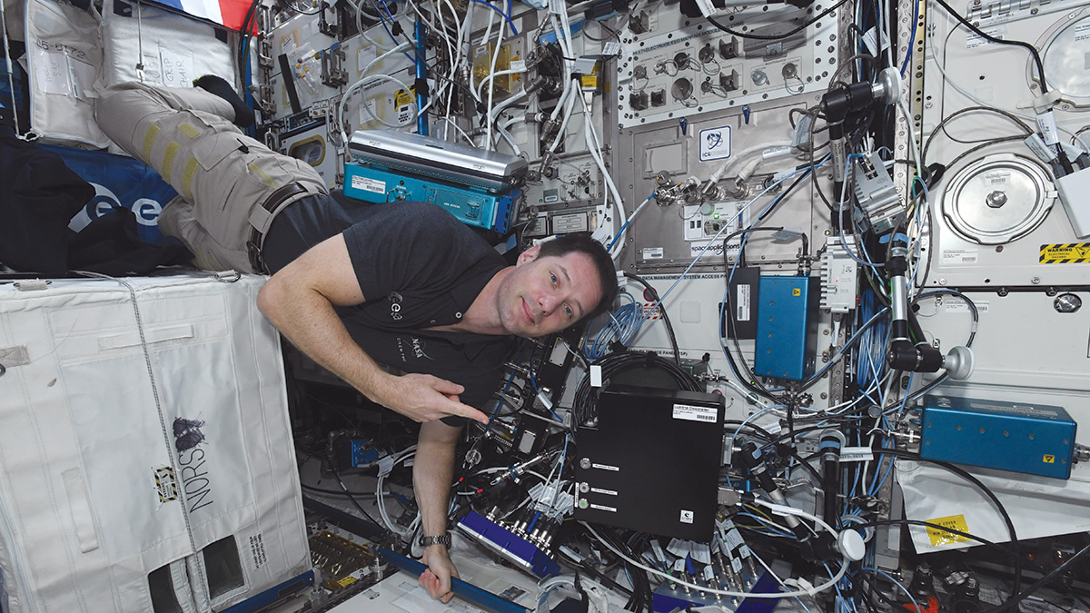
In space, nothing is more important than astronauts’ safety and wellbeing. To this end, in August 2021 ESA astronaut Thomas Pesquet activated the LUMINA experiment inside the International Space Station (ISS), as part of the ALPHA mission (see “Space dosimetry” figure). Developed under the coordination of the French Space Agency and the Laboratoire Hubert Curien at the Université Jean-Monnet-Saint-Étienne and iXblue, LUMINA uses two several-kilometre-long phosphorous-doped optical fibres as active dosimeters to measure ionising radiation aboard the ISS.
When exposed to radiation, optical fibres experience a partial loss of transmitted power. Using a reference control channel, radiation-induced attenuation can be accurately measured related to the total ionising dose, with the sensitivity of the device primarily governed by the length of the fibre. Having studied optical-fibre-based technologies for many years, CERN helped optimise the architecture of the dosimeters and performed irradiation tests to calibrate the instrument, which will operate on the ISS for a period of up to five years.
LUMINA complements dosimetry measurements performed on the ISS using CERN’s Timepix technology – an offshoot of the hybrid-pixel-detector technology developed for the LHC experiments (CERN Courier September/October 2024 p37). Timepix dosimeters have been integrated in multiple NASA payloads since 2012.
5. Radiation-hardness assurance
It’s no mean feat to ensure that CERN’s accelerator infrastructure functions in increasingly challenging radiation environments. Similar challenges are found in space. Damage can be caused by accumulating ionising doses, single-event effects (SEEs) or so-called displacement damage dose, which dislodges atoms within a material’s crystal lattice rather than ionising them. Radiation-hardness assurance (RHA) reduces radiation-induced failures in space through environment simulations, part selection and testing, radiation-tolerant design, worst-case analysis and shielding definition.
Since its creation in 2008, CERN’s Radiation to Electronics project has amplified the work of many equipment and service groups in modelling, mitigating and testing the effect of radiation on electronics. A decade later, joint test campaigns with ESA demonstrated the value of CERN’s facilities and expertise to RHA for spaceflight. This led to the signing of a joint protocol on radiation environments, technologies and facilities in 2019, which also included radiation detectors and radiation-tolerant systems, and components and simulation tools.
Among CERN’s facilities is CHARM: the CERN high-energy-accelerator mixed-field facility, which offers an innovative approach to low-cost RHA. CHARM’s radiation field is generated by the interaction between a 24 GeV/c beam from the Proton Synchrotron and a metallic target. CHARM offers a uniquely wide spectrum of radiation types and energies, the possibility to adjust the environment using mobile shielding, and enough space to test a medium-sized satellite in full operating conditions.
Radiation testing is particularly challenging for the new generation of rapidly developed and often privately funded “new space” projects, which frequently make use of commercial and off-the-shelf (COTS) components. Here, RHA relies on testing and mitigation rather than radiation hardening by design. For “flip chip” configurations, which have their active circuitry facing inward toward the substrate, and dense three-dimensional structures that cannot be directly exposed without compromising their performance, heavy-ion beams accelerated to between 10 and 100 MeV/nucleon are the only way to induce SEE in the sensitive semiconductor volumes of the devices.
To enable testing of highly integrated electronic components, ESA supported studies to develop the CHARM heavy ions for micro-electronics reliability-assurance facility – CHIMERA for short (see “CHIMERA” figure). ESA has sponsored key feasibility activities such as: tuning the ion flux in a large dynamic range; tuning the beam size for board-level testing; and reducing beam energy to maximise the frequency of SEE while maintaining a penetration depth of a few millimetres in silicon.
6. In-orbit demonstrators
Weighing 1 kg and measuring just 10 cm on each side – a nanosatellite standard – the CELESTA satellite was designed to study the effects of cosmic radiation on electronics (see “CubeSat” figure). Initiated in partnership with the University of Montpellier and ESA, and launched in July 2022, CELESTA was CERN’s first in-orbit technology demonstrator.
As well as providing the first opportunity for CHARM to test a full satellite, CELESTA offered the opportunity to flight-qualify SpaceRadMon, which counts single-event upsets (SEUs) and single-event latchups (SELs) in static random-access memory while using a field-effect transistor for dose monitoring. (SEUs are temporary errors caused by a high-energy particle flipping a bit and SELs are short circuits induced by high-energy particles.) More than 30 students contributed to the mission development, partially in the frame of ESA’s Fly Your Satellite Programme. Built from COTS components calibrated in CHARM, SpaceRadMon has since been adopted by other ESA missions such as Trisat and GENA-OT, and could be used in the future as a low-cost predictive maintenance tool to reduce space debris and improve space sustainability.
The maiden flight of the Vega-C launcher placed CELESTA on an atypical quasi-circular medium-Earth orbit in the middle of the inner Van Allen proton belt at roughly 6000 km. Two months of flight data sufficed to validate the performance of the payload and the ground-testing procedure in CHARM, though CELESTA will fly for thousands of years in a region of space where debris is not a problem due to the harsh radiation environment.
The CELESTA approach has since been adopted by industrial partners to develop radiation-tolerant cameras, radios and on-board computers.
7. Stimulating the space economy
Space technology is a fast-growing industry replete with opportunities for public–private cooperation. The global space economy will be worth $1.8 trillion by 2035, according to the World Economic Forum – up from $630 billion in 2023 and growing at double the projected rate for global GDP.
Whether spun off from space exploration or particle physics, ESA and CERN look to support start-up companies and high-tech ventures in bringing to market technologies with positive societal and economic impacts (see “Spin offs” figure). The use of CERN’s Timepix technology in space missions is a prime example. Private company Advacam collaborated with the Czech Technical University to provide a Timepix-based radiation-monitoring payload called SATRAM to ESA’s Proba-V mission to map land cover and vegetation growth across the entire planet every two days.
Advacam is now testing a pixel-detector instrument on JoeySat – an ESA-sponsored technology demonstrator for OneWeb’s next-generation constellation of satellites designed to expand global connectivity. Advacam is also working with ESA on radiation monitors for Space Rider and NASA’s Lunar Gateway. Space Rider is a reusable spacecraft whose maiden voyage is scheduled for the coming years, and Lunar Gateway is a planned space station in lunar orbit that could act as a staging post for Mars exploration.
Another promising example is SigmaLabs – a Polish startup founded by CERN alumni specialising in radiation detectors and predictive-maintenance R&D for space applications. SigmaLabs was recently selected by ESA and the Polish Space Agency to provide one of the experiments expected to fly on Axiom Mission 4 – a private spaceflight to the ISS in 2025 that will include Polish astronaut and CERN engineer Sławosz Uznański (CERN Courier May/June 2024 p55). The experiment will assess the scalability and versatility of the SpaceRadMon radiation-monitoring technology initially developed at CERN for the LHC and flight tested on the CELESTA CubeSat.
In radiation-hardness assurance, the CHIMERA facility is associated with the High-Energy Accelerators for Radiation Testing and Shielding (HEARTS) programme sponsored by the European Commission. Its 2024 pilot user run is already stimulating private innovation, with high-energy heavy ions used to perform business-critical research on electronic components for a dozen aerospace companies.
More than 100 accelerator scientists, engineers and particle physicists gathered in person and remotely at Fermilab from 30 October to 1 November for the first of a new series of workshops to discuss the future of beam-cooling technology for a muon collider. High-energy muon colliders offer a unique combination of discovery potential and precision. Unlike protons, muons are point-like particles that can achieve comparable physics outcomes at lower centre-of-mass energies. The large mass of the muon also suppresses synchrotron radiation, making muon colliders promising candidates for exploration at the energy frontier.
The International Muon Collider Collaboration (IMCC), supported by the EU MuCol study, is working to assess the potential of a muon collider as a future facility, along with the R&D needed to make it a reality. European engagement in this effort crystalised following the 2020 update to the European Strategy for Particle Physics (ESPPU), which identified the development of bright muon beams as a high-priority initiative. Worldwide interest in a muon collider is quickly growing: the 2023 Particle Physics Project Prioritization Panel (P5) recently identified it as an important future possibility for the US particle-physics community; Japanese colleagues have proposed a muon-collider concept, muTRISTAN (CERN Courier July/August 2024 p8); and Chinese colleagues have actively contributed to IMCC efforts as collaboration members.
Lighting the way
The workshop focused on reviewing the scope and design progress of a muon-cooling demonstrator facility, identifying potential host sites and timelines, and exploring science programmes that could be developed alongside it. Diktys Stratakis (Fermilab) began by reviewing the requirements and challenges of muon cooling. Delivering a high-brightness muon beam will be essential to achieving the luminosity needed for a muon collider. The technique proposed for this is ionisation cooling, wherein the phase-space volume of the muon beam decreases as it traverses a sequence of cells, each containing an energy- absorbing material and accelerating radiofrequency (RF) cavities.
Roberto Losito (CERN) called for a careful balance between ambition and practicality – the programme must be executed in a timely way if a muon collider is to be a viable next-generation facility. The Muon Cooling Demonstrator programme was conceived to prove that this technology can be developed, built and reliably operated. This is a critical step for any muon-collider programme, as highlighted in the ESPPU–LDG Accelerator R&D Roadmap published in 2022. The plan is to pursue a staged approach, starting with the development of the magnet, RF and absorber technology, and demonstrating the robust operation of high-gradient RF cavities in high magnetic fields. The components will then be integrated into a prototype cooling cell. The programme will conclude with a demonstration of the operation of a multi-cell cooling system with a beam, building on the cooling proof of principle made by the Muon Ionisation Cooling Experiment.
Chris Rogers (STFC RAL) summarised an emerging consensus that it is critical to demonstrate the reliable operation of a cooling lattice formed of multiple cells. While the technological complexity of the cooling-cell prototype will undergo further review, the preliminary choice presents a moderately challenging performance that could be achieved within five to seven years with reasonable investment. The target cooling performance of a whole cooling lattice remains to be established and depends on future funding levels. However, delegates agreed that a timely demonstration is more important than an ambitious cooling target.
Worldwide interest in a muon collider is quickly growing
The workshop also provided an opportunity to assess progress in designing the cooling-cell prototype. Given that the muon beam originates from hadron decays and is initially the size of a watermelon, solenoid magnets were chosen as they can contain large beams in a compact lattice and provide focusing in both horizontal and vertical planes simultaneously. Marco Statera (INFN LASA) presented preliminary solutions for the solenoid coil configuration based on high-temperature superconductors operating at 20 K: the challenge is to deliver the target magnetic field profile given axial forces, coil stresses and compact integration.
In ionisation cooling, low-Z absorbers are used to reduce the transverse momenta of the muons while keeping the multiple scattering at manageable levels. Candidate materials are lithium hydride and liquid hydrogen. Chris Rogers discussed the need to test absorbers and containment windows at the highest intensities. The potential for performance tests using muons or intensity tests using another particle species such as protons was considered to verify understanding of the collective interaction between the beam and the absorber. RF cavities are required to replace longitudinal energy lost in the absorbers.Dario Giove (INFN LASA) introduced the prototype of an RF structure based on three coupled 704 MHz cavities and presented a proposal to use existing INFN capabilities to carry out a test programme for materials and cavities in magnetic fields. The use of cavity windows was also discussed, as it would enable greater accelerating gradients, though at the cost of beam degradation, increased thermal loads and possible cavity detuning. The first steps in integrating these latest hardware designs into a compact cooling cell were presented by Lucio Rossi (INFN LASA and UMIL). Future work needs to address the management of the axial forces and cryogenic heat loads, Rossi observed.
Many institutes presented a strong interest in contributing to the programme, both in the hardware R&D and hosting the eventual demonstrator. The final sessions of the workshop focused on potential host laboratories.
The event underscored the critical need for sustained innovation, timely implementation and global cooperation
At CERN, two potential sites were discussed, with ongoing studies focusing on the TT7 tunnel, where a moderate-power 10 kW proton beam from the Proton Synchrotron could be used for muon production. Preliminary beam physics studies of muon beam production and transport are already underway. Lukasz Krzempek (CERN) and Paul Jurj (Imperial College London) presented the first integration and beam-physics studies of the demonstrator facility in the TT7 tunnel, highlighting civil engineering and beamline design requirements, logistical challenges and safety considerations, finding no apparent showstoppers.
Jeff Eldred (Fermilab) gave an overview of Fermilab’s broad range of candidate sites and proton-beam energies. While further feasibility studies are required, Eldred highlighted that using 8 GeV protons from the Booster is an attractive option due to the favourable existing infrastructure and its alignment with Fermilab’s muon-collider scenario, which envisions a proton driver based on the same Booster proton energy.
The Fermilab workshop represented a significant milestone in advancing the Muon Cooling Demonstrator, highlighting enthusiasm from the US community to join forces with the IMCC and growing interest in Asia. As Mark Palmer (BNL) observed in his closing remarks, the event underscored the critical need for sustained innovation, timely implementation and global cooperation to make the muon collider a reality.
Forty-five experts from industry and academia met in the magnificent city of Toledo, Spain from 23 to 25 September 2024 for the second workshop on efficient RF sources. Part of the I.FAST initiative on sustainable concepts and technologies (CERN Courier July/August 2024 p20), the event focused on recent advances in energy-efficient technology for RF sources essential to accelerators. Progress in the last two years has been unprecedented, with new initiatives and accomplishments around the world fuelled by the ambitious goals of new, high-energy particle-physics projects.
Out of more than 30 presentations, a significant number featured pulsed, high-peak-power RF sources working at frequencies above 3 GHz in the S, C and X bands. These involve high-efficiency klystrons that are being designed, built and tested for the KEK e–/e+ Injector, the new EuPRAXIA@SPARC_LAB linac, the CLIC testing facilities, muon collider R&D, the CEPC injector linac and the C3 project. Reported increases in beam-to-RF power efficiency range from 15 percentage points for the retrofit prototype for CLIC to more than 25 points (expected) for a new greenfield klystron design that can be used across most new projects.
A very dynamic area for R&D is the search of efficient sources for the continuous wave (CW) and long-pulse RF needed for circular accelerators. Typically working in the L-band, existing devices deliver less than 3 MW in peak power. Solid-state amplifiers, inductive output tubes, klystrons, magnetrons, triodes and exotic newly rediscovered vacuum tubes called “tristrons” compete in this arena. Successful prototypes have been built for the High-Luminosity LHC and CEPC with power efficiency gains of 10 to 20 points. In the case of the LHC, this will allow 15% more power without an impact on the electricity bill; in the case of a circular Higgs factory, this will allow a 30% reduction. CERN and SLAC are also investigating very-high-efficiency vacuum tubes for the Future Circular Collider with a potential reduction of close to 50% on the final electricity bill. A collaboration between academia and industry would certainly be required to bring this exciting new technology to light.
Besides the astounding advances in vacuum-tube technology, solid-state amplifiers based on cheap transistors are undergoing a major transformation thanks to the adoption of gallium-nitride technology. Commercial amplifiers are now capable of delivering kilowatts of power at low duty cycles with a power efficiency of 80%, while Uppsala University and the European Spallation Source have demonstrated the same efficiency for combined systems working in CW.
The search for energy efficiency does not stop at designing and building more efficient RF sources. All aspects of operation, power combination and using permanent magnets and efficient modulators need to be folded in, as described by many concrete examples during the workshop. The field is thriving.
Achieving a theoretical uncertainty of only a few per cent in the measurement of physical observables is a vastly challenging task in the complex environment of hadronic collisions. To keep pace with experimental observations at the LHC and elsewhere, precision computing has had to develop rapidly in recent years – efforts that have been monitored and driven by the biennial High Precision for Hard Processes (HP2) conference for almost two decades now. The latest edition attracted 120 participants to the University of Torino from 10 to 13 September 2024.
All speakers addressed the same basic question: how can we achieve the most precise theoretical description for a wide variety of scattering processes at colliders?
The recipe for precise prediction involves many ingredients, so the talks in Torino probed several research directions. Advanced methods for the calculation of scattering amplitudes were discussed, among others, by Stephen Jones (IPPP Durham). These methods can be applied to detailed high-order phenomenological calculations for QCD, electroweak processes and BSM physics, as illustrated by Ramona Groeber (Padua) and Eleni Vryonidou (Manchester). Progress in parton showers – a crucial tool to bridge amplitude calculations and experimental results – was presented by Silvia Ferrario Ravasio (CERN). Dedicated methods to deal with the delicate issue of infrared divergences in high-order cross-section calculations were reviewed by Chiara Signorile-Signorile (Max Planck Institute, Munich).
The Torino conference was dedicated to the memory of Stefano Catani, a towering figure in the field of high-energy physics, who suddenly passed away at the beginning of this year. Starting from the early 1980s, and for the whole of his career, Catani made groundbreaking contributions in every facet of HP2. He was an inspiration to a whole generation of physicists working in high-energy phenomenology. We remember him as a generous and kind person, and a scientist of great rigour and vision. He will be sorely missed.
Data on strokes is plentiful but fragmented, making it difficult to exploit in data-driven treatment strategies. The toolbox of the high-energy physicist is well adapted to the task. To amplify CERN’s societal contributions through technological innovation, the Unleashing a Comprehensive, Holistic and Patient-Centric Stroke Management for a Better, Rapid, Advanced and Personalised Stroke Diagnosis, Treatment and Outcome Prediction (UMBRELLA) project – co-led by Vall d’Hebron Research Institute and Siemens Healthineers – was officially launched on 1 October 2024. The kickoff meeting in Barcelona, Spain, convened more than 20 partners, including Philips, AstraZeneca, KU Leuven and EATRIS. Backed by nearly €27 million from the EU’s Innovative Health Initiative and industry collaborators, the project aims to transform stroke care across Europe.
The meeting highlighted the urgent need to address stroke as a pressing health challenge in Europe. Each year, more than one million acute stroke cases occur in Europe, with nearly 10 million survivors facing long-term consequences. In 2017, the economic burden of stroke treatments was estimated to be €60 billion – a figure that continues to grow. UMBRELLA’s partners outlined their collective ambition to translate a vast and fragmented stroke data set into actionable care innovations through standardisation and integration.
UMBRELLA will utilise advanced digital technologies to develop AI-powered predictive models for stroke management. By standardising real-world stroke data and leveraging tools like imaging technologies, wearable devices and virtual rehabilitation platforms, UMBRELLA aims to refine every stage of care – from diagnosis to recovery. Based on post-stroke data, AI-driven insights will empower clinicians to uncover root causes of strokes, improve treatment precision and predict patient outcomes, reshaping how stroke care is delivered.
Central to this effort is the integration of CERN’s federated-learning platform, CAFEIN. A decentralised approach to training machine-learning algorithms without exchanging data, it was initiated thanks to seed funding from CERN’s knowledge transfer budget for the benefit of medical applications: now CAFEIN promises to enhance diagnosis, treatment and prevention strategies for stroke victims, ultimately saving countless lives. A main topic of the kickoff meeting was the development of the “U-platform” – a federated data ecosystem co-designed by Siemens Healthineers and CERN. Based on CAFEIN, the infrastructure will enable the secure and privacy preserving training of advanced AI algorithms for personalised stroke diagnostics, risk prediction and treatment decisions without sharing sensitive patient data between institutions. Building on CERN’s expertise, including its success in federated AI modelling for brain pathologies under the EU TRUSTroke project, the CAFEIN team is poised to handle the increasing complexity and scale of data sets required by UMBRELLA.
Beyond technological advancements, the UMBRELLA consortium discussed a plan to establish standardised protocols for acute stroke management, with an emphasis on integrating these protocols into European healthcare guidelines. By improving data collection and facilitating outcome predictions, these standards will particularly benefit patients in remote and underserved regions. The project also aims to advance research into the causes of strokes, a quarter of which remain undetermined – a statistic UMBRELLA seeks to change.
This ambitious initiative not only showcases CERN’s role in pioneering federated-learning technologies but also underscores the broader societal benefits brought by basic science. By pushing technologies beyond the state-of-the-art, CERN and other particle-physics laboratories have fuelled innovations that have an impact on our everyday lives. As UMBRELLA begins its journey, its success holds the potential to redefine stroke care, delivering life-saving advancements to millions and paving the way for a healthier, more equitable future.
The High Luminosity Large Hadron Collider, edited by Oliver Brüning and Lucio Rossi, is a comprehensive review of an upgrade project designed to boost the total event statistics of CERN’s Large Hadron Collider (LHC) by nearly an order of magnitude. The LHC is the world’s largest and, in many respects, most performant particle accelerator. It may well represent the most complex infrastructure ever built for scientific research. The increase in event rate is achieved by higher beam intensities and smaller beam sizes at the collision points.
Brüning and Rossi’s book offers a comprehensive overview of this work across 31 chapters authored by more than 150 contributors. Due to the mentioned complexity of the HL-LHC, it is advisable to read the excellent introductory chapter first to obtain an overview on the various physics aspects, different components and project structure. After coverage of the physics case and the upgrades to the LHC experiments, the operational experiences with the LHC and its performance development are described.
The LHC’s upgrade is a significant project, as evidenced by the involvement of nine collaborating countries including China and the US, a materials budget that exceeds one billion Swiss Francs, more than 2200 years of integrated work, and the complexity of the physics and engineering. The safe operation of the enormous beam intensity represented a major challenge for the original LHC, and will be even more challenging with the upgraded beam parameters. For example, the instantaneous power carried by the circulating beam will be 7.6 TW, while the total beam energy is then 680 MJ – enough energy to boil two tonnes of water. Such numbers should be compared with the extremely low power density of 30 mW/cm3, which is sufficient to quench a superconducting magnet coil and interrupt the operation of the entire facility.
The book continues with descriptions of the two subsystems of greatest importance for the luminosity increase: the superconducting magnets and the RF systems including the crab cavities.
Besides the increase in intensity, the primary factor for instantaneous luminosity gain is obtained by a reduction in beam size at the interaction points (IPs), partly through a smaller emittance but mainly through improved beam optics. This change results in a larger beam in the superconducting quadrupoles beside the IP. To accommodate the upgraded beam and to shield the magnet coils from radiation, the aperture of these magnets is increased by more than a factor of two to 150 mm. New quadrupoles have been developed, utilising the superconductor material Nb3Sn, allowing higher fields at the location of the coils. Further measures include the cancellation of the beam crossing angle during collision by dynamic tilting of the bunch orientation using the superconducting crab cavities that were designed for this special application in the LHC. The authors make fascinating observations, for example regarding the enhanced sensitivity to errors due to the extreme beam demagnification at the IPs: a typical relative error of 10–4 in the strength of the IP quadrupoles results in a significant distortion in beam optics, a so-called beta-beat of 7%.
Chapter eight describes the upgrade to the beam-collimation system, which is of particular importance for the safe operation of high-intensity beams. For ion collimation, halo particles are extracted most efficiently using collimators made from bent crystals.
The book continues with a description of the magnet-powering circuits. For the new superconducting magnets CERN is using “superconducting links” for the first time: cable sets made of a high-temperature superconductor that can carry enormous currents on many circuits in parallel in a small cross section; it suffices to cool them to temperatures of around 20 to 30K with gaseous helium by evaporating some of the liquid helium that is used for cooling the superconducting magnets in the accelerator.
Magnetic efforts
The next chapters cover machine protection, the interface with the detectors and the cryogenic system. Chapter 15 is dedicated to the effects of beam-induced stray radiation, in particular on electronics – an effect that has become quite important at high intensities in recent years. Another chapter covers the development of an 11 Tesla dipole magnet that was intended to replace a regular superconducting magnet, thereby gaining space for additional collimators in the arc of the ring. Despite considerable effort, this programme was eventually dropped from the project because the new magnet technology could not be mastered with the required reliability for routine operation; and, most importantly, alternative collimation solutions were identified.
Other chapters describe virtually all the remaining technical subsystems and beam-dynamics aspects of the collider, as well as the extensive test infrastructure required before installation in the LHC. A whole chapter is dedicated to high-field-magnet R&D – a field of utmost importance to the development of a next-generation hadron collider beyond the LHC.
Brüning and Rossi’s book will interest accelerator physicists in that it describes many outstanding beam-physics aspects of the HL-LHC. Engineers and readers with an interest in technology will also find many technical details on its subsystems.
Findable. Accessible. Interoperable. Reusable. That’s the dream scenario for scientific data and tools. The European Open Science Cloud (EOSC) is a pan-European initiative to develop a web of “FAIR” data services across all scientific fields. EOSC’s vision is to put in place a system for researchers in Europe to store, share, process, analyse and reuse research outputs such as data, publications and software across disciplines and borders.
EOSC’s sixth symposium attracted 450 delegates to Berlin from 21 to 23 October 2024, with a further 900 participating online. Since its launch in 2017, EOSC activities have focused on conceptualisation, prototyping and planning. In order to develop a trusted federation of research data and services for research and innovation, EOSC is being deployed as a network of nodes. With the launch during the symposium of the EOSC EU node, this year marked a transition from design to deployment.
While EOSC is a flagship science initiative of the European Commission, FAIR concerns researchers and stakeholders globally. Via the multiple projects under the wings of EOSC that collaborate with software and data institutes around the world, a pan-European effort can be made to ensure a research landscape that encourages knowledge sharing while recognising work and training the next generation in best practices in research. The EU node – funded by the European Commission, and the first to be implemented – will serve as a reference for roughly 10 additional nodes to be deployed in a first wave, with more to follow. They are accessible using any institutional credentials based on GÉANT’s MyAccess or with an EU login. A first operational implementation of the EOSC Federation is expected by the end of 2025.
A thematic focus of this year’s symposium was the need for clear guidelines on the adaption of FAIR governance for artificial intelligence (AI), which relies on the accessibility of large and high-quality datasets. It is often the case that AI models are trained with synthetic data, large-scale simulations and first-principles mathematical models, although these may only provide an incomplete description of complex and highly nonlinear real-world phenomena. Once AI models are calibrated against experimental data, their predictions become increasingly accurate. Adopting FAIR principles for the production, collection and curation of scientific datasets will streamline the design, training, validation and testing of AI models (see, for example, Y Chen et al. 2021 arXiv:2108.02214).
EOSC includes five science clusters, from natural sciences to social sciences, with a dedicated cluster for particle physics and astronomy called ESCAPE: the European Science Cluster of Astronomy and Particle Physics. The future deployment of the ESCAPE Virtual Research Environment across multiple nodes will provide users with tools to bring together diverse experimental results, for example, in the search for evidence of dark matter, and to perform new analyses incorporating data from complementary searches.
Muon radiography – muography for short – uses cosmic-ray muons to probe and image large, dense objects. Coordinated by editors Paola Scampoli and Akitaka Ariga of the University of Bern, the authors of this book provide an invaluable snapshot of this booming research area. From muon detectors, which differ significantly from those used in fundamental physics research, to applications of muography in scientific, cultural, industrial and societal scenarios, a broad cross section of experts describe the physical principles that underpin modern muography.
Hiroyuki Tanaka of the University of Tokyo begins the book with historical developments and perspectives. He guides readers from the first documented use of cosmic-ray muons in 1955 for rock overburden estimation, to current studies of the sea-level dynamics in Tokyo Bay using muon detectors laid on the seafloor and visionary ideas to bring muography to other planets using teleguided rovers.
Scattering methods
Tanaka limits his discussion to the muon-absorption approach to muography, which images an object by comparing the muon flux before and after – or with and without – an object. The muon-scattering approach, which was invented two decades ago, instead exploits the deflection of muons passing through matter that is due to electromagnetic interactions with nuclei. The interested reader will find several examples of the application of muon scattering in other chapters, particularly that on civil and industrial applications by Davide Pagano (Pavia) and Altea Lorenzon (Padova). Scattering methods have an edge in these fields thanks to their sensitivity to the atomic number of the materials under investigation.
Peter Grieder (Bern), who sadly passed away shortly before the publication of the book, gives an excellent and concise introduction to the physics of cosmic rays, which Paolo Checchia (Padova) expands on, delving into the physics of interactions between muons and matter. Akira Nishio (Nagoya University) describes the history and physical principles of nuclear emulsions. These detectors played an important role in the history of particle physics, but are not very popular now as they cannot provide real-time information. Though modern detectors are a more common choice today, nuclear emulsions still find a niche in muography thanks to their portability. The large accumulation of data from muography experiments requires automatic analysis, for which dedicated scanning systems have been developed. Nishio includes a long and insightful discussion on how the nuclear-emulsions community reacted to supply-chain evolution. The transition from analogue to digital cameras meant that most film-producing firms changed their core business or simply disappeared, and researchers had to take a large part of the production process into their own hands.
Fabio Ambrosino and Giulio Saracino of INFN Napoli next take on the task of providing an overview of the much broader and more popular category of real-time detectors, such as those commonly used in experiments at particle colliders. Elaborating on the requirements set by the cosmic rate and environmental factors, their
chapter explains why scintillator and gas-based tracking devices are the most popular options in muography. They also touch on more exotic detector options, including Cherenkov telescopes and cylindrical tracking detectors that fit in boreholes.
In spite of their superficial similarity, methods that are common in X-ray imaging need quite a lot of ingenuity to be adapted to the context of muography. For example, the source cannot be controlled in muography, and is not monochromatic. Both energy and direction are random and have a very broad distribution, and one cannot afford to take data from more than a few viewpoints. Shogo Nagahara and Seigo Miyamoto of the University of Tokyo provide a specialised but intriguing insight into 3D image reconstruction using filtered back-projection.
A broad cross section of experts describe the physical principles that underpin modern muography
Geoscience is among the most mature applications of muography. While Jacques Marteau (Claude Bernard University Lyon 1) provides a broad overview of decades of activities spanning from volcano studies to the exploration of natural caves, Ryuichi Nishiyama (Tokyo) explores recent studies where muography provided unique data on the shape of the bedrock underneath two major glaciers in the Swiss Alps.
One of the greatest successes of muography is the study of pyramids, which is given ample space in the chapter on archaeology by Kunihiro Morishima (Nagoya). In 1971, Nobel-laureate Luis Alvarez’s team pioneered the use of muography in archaeology during an investigation at the pyramid of Khafre in Giza, Egypt, motivated by his hunch that an unknown large chamber could be hiding in the pyramid. Their data convincingly excluded that possibility, but the attempt can be regarded as launching modern muography (CERN Courier May/June 2023 p32). Half a century later, muography was reintroduced to the exploration of Egyptian pyramids thanks to ScanPyramids – an international project led by particle-physics teams in France and Japan under the supervision of the Heritage Innovation and Preservation Institute. ScanPyramids aims at systematically surveying all of the main pyramids in the Giza complex, and recently made headlines by finding a previously unknown corridor-shaped cavity in Khufu’s Great Pyramid, which is the second largest pyramid in the world. To support the claim, which was initially based on muography alone, the finding was cross-checked with the more traditional surveying method based on ground penetrating radar, and finally confirmed via visual inspection through an endoscope.
Pedagogical focus
This book is a precious resource for anyone approaching muography, from students to senior scientists, and potential practitioners from both academic and industrial communities. There are some other excellent books that have already been published on the same topic, and that have showcased original research, but Cosmic Ray Muography’s pedagogical focus, which prioritises the explanation of timeless first principles, will not become outdated any time soon. Given each chapter was written independently, there is a certain degree of overlap and some incoherence in terminology, but this gives the reader valuable exposure to different perspectives about what matters most in this type of research.
To provide the best experiences, we use technologies like cookies to store and/or access device information. Consenting to these technologies will allow us to process data such as browsing behavior or unique IDs on this site. Not consenting or withdrawing consent, may adversely affect certain features and functions.
Functional
Always active
The technical storage or access is strictly necessary for the legitimate purpose of enabling the use of a specific service explicitly requested by the subscriber or user, or for the sole purpose of carrying out the transmission of a communication over an electronic communications network.
Preferences
The technical storage or access is necessary for the legitimate purpose of storing preferences that are not requested by the subscriber or user.
Statistics
The technical storage or access that is used exclusively for statistical purposes.The technical storage or access that is used exclusively for anonymous statistical purposes. Without a subpoena, voluntary compliance on the part of your Internet Service Provider, or additional records from a third party, information stored or retrieved for this purpose alone cannot usually be used to identify you.
Marketing
The technical storage or access is required to create user profiles to send advertising, or to track the user on a website or across several websites for similar marketing purposes.