Comsol -leaderboard other pages

Topics

CMS installs the world’s largest silicon detector

insertion of the CMS microstrip tracker

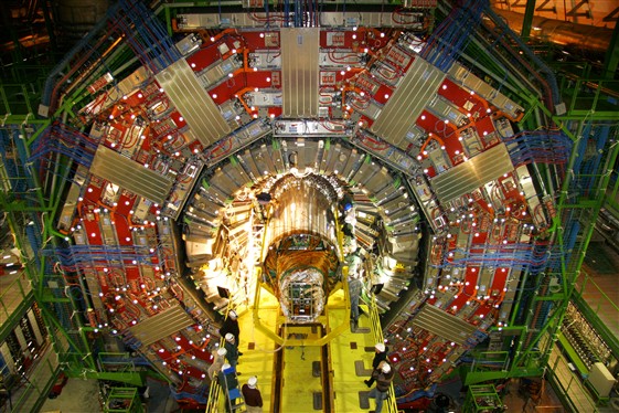
In December 1999 the CMS collaboration made the daring decision to change its tracking detector from a design that included gaseous detectors to one constructed entirely from silicon sensors, using both microstrip and pixel technology. On 15 December 2007, teams working in the cavern at Point 5 on the LHC installed the microstrip tracking system into the experiment. The pixel detector will soon follow, completing the CMS Tracker and marking the culmination of eight years of careful work to design, prototype, construct and commission the largest silicon detector ever built.

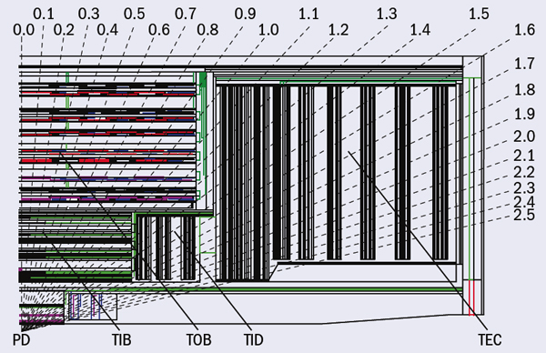
The collaboration envisaged a tracking system 40 times larger than any existing silicon detector system, with a performance comparable to the vertex detectors used at LEP. The detector would house about 205 m2 of silicon sensors (approximately the area of a tennis court) comprising 9.3 million microstrips and 66 million pixels. The aim was to achieve a precision of about 10 μm in spatial and vertex reconstruction resolutions – enough for excellent identification of heavy flavour hadrons – and excellent momentum measurement over a wide momentum range at the LHC. The readout would require 73,000 radiation-hard, low-noise microelectronics chips, almost 40,000 analogue optical links, 1000 power supply units and 500 off-detector readout and control modules. The complete system would be constructed in two halves from nine separate subdetector units: two each of microstrip inner barrels, outer barrels and endcaps, three pixel units in the form of a barrel system and two identical forward units.

diagram of a quarter of the detector

In June 2000, the LHC Committee approved the Technical Design Report for the new design and the project formally got underway. A collaboration of more than 500 physicists and engineers from 51 institutions based in Austria, Belgium, Finland, France, Germany, Italy, Switzerland, the UK and the US, as well as from CERN, took joint responsibility for the project. They agreed that the inner barrel would be constructed by an Italian consortium, the outer barrel system by CERN together with Finnish and US groups, and the two endcaps by European teams. Swiss groups would build the central barrel region of the pixel system and a US collaboration would provide the forward pixel units.

The assembly project
The detailed design of each of the subdetector units took several years, including extensive testing of prototype sensors, modules and the readout, cooling and power systems. Production of the microstrip detector modules began in November 2004 using the sensors, hybrids and electronic components developed during the earlier phase – all of which had been thoroughly studied and evaluated to ensure maximum reliability and performance. Production of these modules was complete by March 2006. Then, after further substantial testing and thermal cycling, they were ready for mounting onto low-mass carbon fibre substructures with pre-assembled cooling circuits.

The project also became a massive worldwide logistical activity. The microstrip sensors were manufactured in Japan, with contributions from Italian industry, and shipped to Europe and the US for evaluation. The sensors were then moved to other European and US destinations for construction into modules using customized automated assembly equipment that CMS engineers had devised; and they journeyed further still for assembly into sub-units such as rods for the outer barrel, shells and discs for the inner barrel, and petals for the endcaps. The pixel system involved a similar transporting of parts, starting with commercially manufactured sensors from Norway.

The electronic readout system relied on developments in radiation-hard electronics and innovations in optical links, technologies that evolved rapidly in the 1990s. The CMS system culminated with the APV25 – the first large readout chip for a particle-physics experiment to use 0.25 μm CMOS integrated circuit technology – and novel analogue fibre-optic links. Much of this development was the responsibility of groups in the UK and teams at CERN, who worked closely with other CMS groups to assemble the elements of the readout system. CERN designed a set of control and ancillary chips using 0.25 μm CMOS technology, extensively exploited both in the Tracker and throughout CMS.

The collaboration also subcontracted a great deal of the assembly work to industries in several countries, including Austria, France, Italy, Japan, Switzerland and the UK

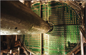
The automated assembly pioneered for this enormous system was vital for constructing thousands of modules quickly, so that the 15,200 required could be delivered on time. It also generated a huge interconnection requirement. Each module was assembled from one or two microstrip sensors, which had to be connected to the APV25 readout chip. The module chips also had to be bonded to their low-mass carrier. The intensive use of automatic-wire bonders met this demand and maintained consistent throughput with few delays, despite occasional variations in bond quality and rejection of sub-optimal modules.

The collaboration also subcontracted a great deal of the assembly work to industries in several countries, including Austria, France, Italy, Japan, Switzerland and the UK. In partnership with CMS institutes, the companies manufactured components and produced electronics boards, mounting and aligning semiconductor lasers, optical fibres, photodiodes, and analogue and digital electronics, including field-programmable gate arrays that were then state of the art. All modules were thoroughly tested in industry – often using CMS-constructed test equipment – then re-tested for acceptance in CMS laboratories. It is impossible here to do justice to the efforts of the CMS institutes, all of which took on significant tasks in assembly, evaluation and procurement.

Collaboration members constructed new facilities in many institutions for assembling the subdetectors, as well as expanding and utilizing large laboratories such as at CERN, Fermilab and Pisa. Aachen assembled one of the Tracker endcaps, while Florence, Pisa and Torino jointly integrated the inner barrels and discs. There were intensive reviews at all system levels for each stage of production and integration to ensure that quality and performance were maintained.

microstrip tracker

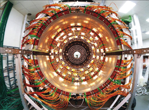
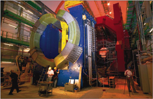
On the main CERN site, CMS built a facility to assemble the final detector and to provide an environment where a substantial fraction of it could be fully commissioned before final installation into CMS at Point 5. The Tracker Integration Facility is a 350 m2 class 100,000 cleanroom, which was also used to integrate the entire outer-barrel system and the second endcap. Each subdetector underwent testing and thermal cycling before transportation to CERN. Further acceptance tests took place after arrival before final integration into the support structure.

The two halves of the outer barrel were built inside the Tracker support tube, which is a low-mass carbon fibre cylinder 5.4 m long and 2.5 m in diameter. The outer-barrel subdetector was completed in November 2006. The inner-barrel halves arrived at CERN in April and September 2006 for final testing before insertion into the outer barrel. The first half section was placed in position in December 2006 and the second half inner barrel and the endcap followed rapidly, with integration of the second endcap completed on 22 March 2007.

As each subdetector was assembled, the teams re-tested it to ensure that it continued to achieve the required performance. The integration facility included rack-mounted electronics, cooling and air-conditioning, which allowed the Tracker to observe cosmic-ray events before installation underground. This incorporated a quarter of the complete safety, control, power, data-acquisition and computing systems for the Tracker – destined eventually for the CMS caverns – including electrical and optical cables, which were to be re-used to keep down costs.

From March until August 2007, all aspects of the Tracker underwent testing, including safety, control and monitoring systems.Several million cosmic-ray events were recorded at five operating temperatures ranging between –15 °C and +15 °C. The data were reconstructed using the CMS-distributed computing Grid and were analysed throughout the world. All systems operated reliably during this five-month period and the collaboration verified that the assembled detector met the performance specifications.

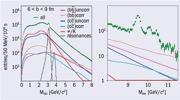
Analysis of the cosmic-ray data shows that the performance of the microstrip tracker is excellent. The number of inactive strips is below one part in 2000; noisy strips do not exceed 0.5%. The signal-to-noise ratio, which depends on sensor thickness, was about 28 for 300 μm sensors. Measurements showed the track cluster finding efficiency to be better than 99.8%. All of these results meet or exceed expectations, which bodes well for LHC physics.

Final installation
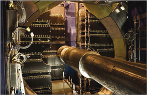
At the CMS experimental area at Point 5, preparation for installing the Tracker began before the solenoid magnet was even lowered into the cavern in February 2007. Installation and testing of the cooling plants, power systems and off-detector readout electronics, as well as control and data-acquisition systems took place throughout 2007.

The final performance of the subdetectors in LHC collisions is crucially dependent on the electrical quality of the underground environment, which will only become fully understood after the experiment is complete. The Tracker’s electronics are exquisitely sensitive to tiny signals and must be protected against unwanted noise. To achieve this, 32 interconnection units (patch panels) serving different sectors of the Tracker were installed at the edge of the CMS solenoid, through which all electrical power and cooling services – as well as optical fibres and monitoring wires – pass. The patch panels filter electronic noise and will permit in situ optimization of the detector’s grounding. They also provide termination for cooling, optical links and electrical cables so that all services could be tested as far as possible in CMS before the Tracker arrived.

By late September 2007, the installation teams had completed the massive task of installing cooling systems for 450 loops, 2300 power and 400 fibre-optic cables. The microstrip tracker was transported overnight to Point 5 on 12 December and installation into CMS was completed over the following two days. Connection of the services from the patch panels to the Tracker, and commissioning the Tracker with the rest of CMS, will be completed this spring.

The pixel system
Although a physically smaller device, the pixel system has about a factor of seven more channels. Being at the centre of the detector, concern about minimum material budget and higher radiation levels necessitates even greater attention. Interconnection technologies – especially fine-pitch bump bonding, which were not yet mature for applications in particle physics – had to be studied and, in some cases, developed in CMS labs to allow construction of the detector. The pixel assembly project followed a similar course to the microstrip tracker, with significant transport of parts around the world. Fermilab was at the centre of US activity, and was where the final assembly of the forward system was completed following plaquette construction at Purdue University. The team at the Paul Scherrer Institute (PSI) assembled the barrel subdetector with the collaboration of Swiss universities. PSI also designed the pixel readout chip, while other chips were developed in PSI and the US; the pixel detectors have also exploited components from the microstrip tracker.

The pixel system is scheduled for insertion into CMS following the installation and bake out of the LHC beam pipe in April. The complete forward subdetector was transported to CERN from Fermi-lab in December 2007 and is now undergoing extensive system tests at the Tracker Integration Facility. The barrel subdetector is also complete and currently being commissioned at PSI. It will be transported to CERN in April.

Construction of IceCube project at the South Pole reaches the halfway point

The teams installing the IceCube experiment at the South Pole have completed a highly successful austral summer season, during which they installed 18 detector strings – 4 more than in the baseline plan. This marks the halfway point in the construction of the neutrino telescope, which will detect extraterrestrial neutrinos with energies of above 1 TeV.

Not only has the team exceeded the 2007/08 baseline plan, they also finished the deployment ahead of schedule. This means that there is plenty of time to prepare the site for next year’s season, and suggests that construction of the detector will be complete in three more seasons, as currently planned. Meanwhile, the detector will reach an exposure of a km2-year within two years – a long-anticipated milestone of neutrino astronomy.

IceCube now consists of 40 strings, each instrumented with 60 digital optical modules (DOMs). The drilling and deployment teams were able to make holes 2500 km deep in the Antarctic ice and lower the detector strings at the rate of about one every 50 hours. IceCube now has a volume of half a cubic kilometre.

The last members of the IceCube construction team were due to leave on 15 February, after which the IceCube winter team would take over the job of incorporating the new DOMs into the data acquisition system. The researchers are evaluating each DOM to determine that it survived the deployment and “freeze-in” process. There are now 2400 DOMs in the ice at the South Pole, and in February, 99% of the DOMs that had been powered were working.

In addition to deploying the strings, this season the teams also installed a further 28 tanks for the IceTop array, a surface array to detect high-energy cosmic rays and to provide a veto for air showers that interfere with neutrino detection within IceCube.

• IceCube is an international effort involving 28 institutions and is funded by the US National Science Foundation, with significant contributions from Germany, Sweden, Belgium, Japan, New Zealand, the Netherlands and Switzerland.

The team at SPIN@COSY looks inside a spin resonance

The SPIN@COSY polarized-beam team has found striking new results while studying the spin-manipulation of polarized deuterons at the Cooler Synchrotron (COSY) at the Forschungszentrum in Jülich. The team – from Michigan, COSY, Bonn, the Japan Proton Accelerator Research Complex (J-PARC), Indiana and Groningen, led by Michigan’s Alan Krisch – used a new RF-solenoid magnet to manipulate the spins of stored 1.85 GeV/c deuterons (spin-1 bosons).

CCnew3_02_08

Maria Leonova, a graduate student at Michigan, and Alexander Schnase, an electrical engineer at J-PARC, designed the new RF-solenoid, which was built by Dieter Prasuhn and his accelerator team at COSY. It used the same sophisticated RF high-voltage supply as its predecessor, an RF-dipole. However, the RF solenoid produces a longitudinal RF magnetic field rather than a radial field.

The goal of the experiment was to test precisely a new analytic matrix formalism developed by Alexander Chao of SLAC, a theoretical member of the SPIN@COSY team (Chao 2005). The Chao formalism is the first generalization of the famed Froissart–Stora formula, which allows the calculation of the beam polarization after passing through a spin resonance (Froissart and Stora 1960). This formula is valid only if the initial beam polarization is measured long before crossing the spin resonance and the final beam polarization long after crossing it. As polarized beam hardware and the understanding of spin dynamics improved, however, polarized beam enthusiasts became eager to learn what happens very near or even inside a spin resonance.

CCnew4_02_08

Vasily Morozov at Michigan used the Chao formalism to calculate in detail what might happen in a new type of experiment, where a 1 MHz RF-magnet’s frequency is swept by a fixed range of 400 Hz, while its end-frequency fend steps through many different values near and inside an RF spin resonance (figure 2). The Chao–Morozov calculations predicted that, if the magnet’s resonance strength ε was not high enough to flip the spin fully, then there would be large oscillations in the final polarization. These oscillations seem so sensitive to ε and other parameters, such as the beam’s momentum spread, Δp/p, and the resonance’s central frequency fr, that the oscillations might provide a new way to measure such parameters precisely.

CCnew5_02_08

The data from the new experiment showed striking oscillations that agree very well with these calculations (figure 3). The experiment’s data also verified the polarization’s extreme sensitivity to the resonance’s strength, ε, the resonance’s frequency spread, δfΔp, (owing to the beam’s momentum spread, Δp/p), and the resonance’s central frequency fr. Moreover, the data clearly demonstrate that the oscillations’ size increased rapidly as the beam’s momentum spread decreased (Morozov et al. 2007 and 2008).

These new experimental results also confirm the validity of the Chao matrix formalism. It may now be used to understand better the behaviour of the 100–250 GeV polarized protons stored in RHIC at Brookhaven and, perhaps in the future, polarized antiprotons in the Facility for Antiproton and Ion Research at GSI (see FAIR gets the green light at GSI), or polarized protons stored in J-PARC or even in the LHC at CERN.

Vertex 2007 prepares for the radiation challenge

The use of precision position information at the level of a few micrometres has become an increasingly important part of high-energy physics experiments. The purpose of the annual International Workshop on Vertex Detectors is to review progress on silicon-based vertex detectors, investigate the possibilities of new materials and design structures, and discuss applications to medical and other fields. More than 70 physicists participated in the 16th meeting in the series, which was held at the Crowne Plaza Hotel in Lake Placid, New York, on 23–28 September and hosted by the high-energy physics group of Syracuse University. Lake Placid provided a splendid venue (at the height of the autumn tree colours) and created an inspiring atmosphere for excellent talks and discussions. The workshop also included a new poster session to showcase the work of bright young researchers.

CCver1_01_08

The programme included extensive reviews of the almost completed systems for the major LHC experiments – ALICE, ATLAS, CMS and LHCb. The talks and informal discussions showed the great progress there has been in commissioning these impressive systems with test beams and cosmic rays. As the experiments gear up for data-taking, the teams are validating and refining the tracking, alignment and vertex-reconstruction software tools. There are, however, concerns about exposing these detectors at frighteningly close distances to the beams in an accelerator that has not yet run. There were presentations of plans for experiment protection at the LHC, but the information provided did not quell the debate.

While everyone is eagerly awaiting data-taking at the LHC, there are already plans for upgrades and new facilities. The world community is poised to meet the challenges of vertex detectors for the proposed International Linear Collider, high-luminosity upgrades of the LHC – the Super LHC (SLHC) – and flavour physics experiments (a Super B-factory and an upgrade of the LHCb experiment). Many upgrade paths require vertex detectors with improved radiation hardness and higher segmentation to cope with the higher multiplicities and higher event rates. In addition, several considerations, not the least of which is the amount of material, motivate the effort towards detector thinning.

Upgraded experiments will also require upgraded analysis tools. Many important new particles, such as Higgs bosons, are likely to decay into B particles. These leave displaced vertices, so algorithms that provide this information, especially in the earlier stages of the trigger processor, will be necessary. This is a paramount consideration in the LHCb upgrade and provides a strong motivation to pursue a pixel-based vertex detector.

CCver2_01_08

Novel devices

A strong focus of this workshop centred on the evaluation of new devices developed to address a variety of the challenges posed by future projects. Radiation hardness, for example, is a critical consideration for SLHC upgrades. This is the motivation behind RD50, a large R&D effort based at CERN that involves scientists from all over the world. After years of R&D on a variety of technologies and structures, this group is now reaching important conclusions. In particular, devices using “n+” electrodes (pixels or strips) implanted on p-type substrates appear to be one of the most effective options to cope with increased radiation fluence. Speakers presented recent results and showed that microstrip detectors can still be operated after being irradiated at fluencies up to 1016 neutrons/cm2, as required in the innermost layers at SLHC luminosities (figure 1). One plane of a strip-detector implemented on p-type substrates has been installed in LHCb, “the first full-scale SLHC silicon plane”. Although the traditional emphasis of this conference is on silicon-based technology, discussions also covered the naturally radiation-hard diamond detectors, in particular the promising single-crystal diamond devices.

The reduced collection distance achievable at high levels of irradiation has helped to inspire renewed interest in thinned silicon. The workshop learned that this performs just as well as “thick” 300-μm detectors after sufficient radiation, as the charge cannot be collected out of the thicker sensors. In addition, examples were shown of detectors thinned down to 10 μm that are functional and mechanically stable. Other novel detector concepts included 3-dimensional detectors; monolithic devices, where the readout chip is made on the same silicon substrate as used for the sensor; and DEPFET, where each pixel is a p-channel FET on a completely depleted bulk. Another interesting development is the so-called “3D integration”, featuring integration of the sensor and several layers of readout electronics, which is facilitated by the strong push towards miniaturization in the computer industry.

Silicon micropattern detectors are central to precision imaging in several areas of research, from medicine to biology, to astrophysics and astroparticle physics. The field is in rapid evolution and several interesting talks highlighted a broad spectrum of applications. Examples of imaging geared towards medical or biological applications included the MEDIPIX chip, 3H imaging, NANO-CT scanning, and the PILATUS system – a pixelated hybrid silicon X-ray detector developed for protein crystallography at the Swiss Light Source. Astrophysics applications included PAMELA, now taking data in space, and the more futuristic EXIST, a proposed large-area telescope for X-ray astronomy.

• The next meeting in the series will be run by Richard Brenner and held near Stockholm in the summer.

Electronics for LHC-era experiments and beyond

The Topical Workshop on Electronics for Particle Physics (TWEPP ’07) recently brought together more than 160 participants from the international high-energy physics community, specialized technical institutes and industry. Held in Prague on 3–7 September 2007, the workshop was organized by Charles University, the Czech Technical University, the Institute of Physics and the Nuclear Physics Institute of the Czech Academy of Sciences. It represented both a continuation and a significant broadening of the scope of the series of annual Workshops on Electronics for LHC Experiments initiated in 1994.

CClhc1_01_08

This series of workshops began within the framework of the R&D programme supervised initially by CERN’s Detector Research and Development Committee and later by the LHC Committee. The goal was to promote collaboration and dissemination of relevant expertise within the LHC community, harness specialized knowledge from industry and technical institutes and encourage common approaches and the adoption of standards. The proceedings of the previous 12 workshops show that the programme met these aims. Overall progress has often been spectacular, from the initial R&D phase to the installation and commissioning of the large-scale and complex high-technology electronics systems for LHC experiments. Despite the successful resolution of the many initial R&D challenges, several practical electrical engineering aspects have recently proved to cause some of the biggest headaches in assembling the full LHC detector systems.

With the LHC experiments now well into their commissioning phase, the meeting in Prague was a timely occasion to review lessons learned from more than a decade of design, production and installation of detector electronics. It was also a time to look forward to the challenges of developments in electronics for potential experimental facilities beyond the LHC, such as the Super-LHC (SLHC), the International Linear Collider (ILC) and the Compact Linear Collider study, as well as neutrino and fixed-target experiments. The workshop featured 89 submitted presentations, nine invited talks, topical sessions on supply and distribution of power in detectors, working groups on microelectronics and optoelectronics, and an optional tutorial on robust ASIC designs for hostile environments. While the majority of contributions (58%) described electronics for LHC experiments, 9% of the papers addressed an SLHC upgrade issue and 33% concerned the ILC or other experiments. Some 16% of participants were from non-European institutes.

CClhc2_01_08

Some lessons learnt

Approximately 40% of the workshop contributions were on electronics systems, installation and commissioning. This is no surprise given the advanced state of the LHC experiments. Speakers reported on significant progress in integrating the sub-detectors in the LHC experiments and in commissioning tests with cosmic rays. In general, the performance of the front-end and back-end electronics and the associated software and firmware for controls, monitoring and readout, agrees well with expectations. This major achievement is largely a result of the tremendous effort that the community has made to deliver complex and functional electronics systems to the experiments. However, installation and verification of the complicated services for the front-end electronics (power, cooling, cables etc) often turned out to be much more difficult than anticipated. One particular point of concern relates to the supply and distribution of power to the experiments. In the current LHC detectors, typically only around 30–40% of the power produced is really dissipated in the front-end circuits, the remainder being lost in long power cables and through conversion inefficiencies in power supplies.

A more efficient power distribution system would have reduced the amount of material required in the form of power cabling and cooling infrastructure to remove the heat; this in turn would have allowed improved tracking detectors. The development of such power supply and distribution systems will be critical for the successful construction of future detectors. In a possible SLHC luminosity upgrade, for example, a 10-fold increase in luminosity will require detectors with higher granularity and hence an increased number of electronic channels. The use of advanced front-end ASIC technology holds the promise of reduced power dissipation per channel, and therefore should help to contain any increase in the global power dissipation of the whole front-end electronics systems. Nevertheless, these advanced IC technologies operate at lower voltages than those employed in the LHC detectors today, so the fraction of power dissipated in power cabling at the SLHC detectors is at risk of increasing.

To review the present situation and discuss future orientations, the workshop devoted a day to topical sessions on power management and distribution in large detector systems, with presentations and discussions about several new approaches. At the ILC for instance, the time structure with bunch trains of around 1 ms interspersed with 200 ms of idle time offers the possibility of placing the electronics in quiescent mode during the idle periods, which could lead to a 99% reduction in the average power consumed by the front-end electronics. This power cycling technique cannot be used at the SLHC, but local DC–DC conversion and serial powering are strong alternative options. The first of these alternative approaches delivers power to the front-end modules at high voltage (say, 24 V) and then uses a local DC–DC converter to step down to the required ASIC supply voltage (1.5 V for 130 nm CMOS). In the serial-powering approach the floating modules are powered in series and fed with a constant current. Each module is equipped with a voltage regulator and a current shunt in order to maintain the required drop in supply voltage, regardless of load variations or possible module failure.

The topical sessions concluded with general agreement on the need to adopt a coordinated approach to the supply, management and distribution of power for large experiments in order to avoid a posteriori systems engineering. A working group will be established to assess power-related issues, including lessons learnt from LHC detectors; power management developments required for future upgrades and experiments; and methodologies for the quality control and qualification of power systems.

Front-end to back-end

The second largest session of the workshop focused on ASIC developments. In view of the considerable challenge presented by electronics for the future SLHC or ILC detectors, clear signs of vigorous development activity are excellent news. The ASIC session covered a rich set of applications, including front-end circuits for pixel and micro-strip detectors for tracking, front-end electronics for calorimetry at the LHC, SLHC and ILC, and generic functions, such as single-event upset-tolerant programmable logic and optical transfer of data, clock and trigger signals at multi-gigabit rates. ASIC projects presented at the workshop employed a range of standard CMOS technologies (with minimum feature sizes of 350 nm, 250 nm, 180 nm and 130 nm), as well as other technologies chosen to meet the specific requirements of different detectors. The latter included silicon-germanium processes to handle signals with a wide dynamic range, high-voltage processes for DC–DC converter developments, and silicon-on-insulator technology for the development of monolithic integrated pixel detectors.

A large fraction of the contributions on ASICs were related to the ILC detectors, where a low material budget within the detector and low-power front-end electronics are particularly important. Developments addressing these requirements include monolithic pixel systems, ASICs to read out CCD arrays and ASICs to read out silicon microstrips in advanced 130 nm CMOS technology with built-in support for power cycling.

The ASICs being developed for particle detector readout are now becoming real “systems on chips”, and their increasing complexity requires ever more expertise from larger and larger development teams, as well as an approach that takes system aspects into account from an early stage of the development. The appropriate choice of technology will depend strongly on the specific development timescale of the different projects, as well as the global cost of accessing such technologies, including qualification and the design support environment. The use of a common technology base would allow sharing of building blocks and reduction of the global effort needed for radiation hardness qualification.

The maintenance of the firmware and the software will present a considerable support challenge over the lifetime of the experiments.

A Microelectronics Users’ Group meeting directly followed the ASIC session to spread information about progress in making deep sub-micrometre technologies available to the particle-physics community. CERN has negotiated access to 130 nm and 90 nm CMOS technologies following a similar model to that used for the 250 nm technology employed in many of the developments for LHC experiments. A design kit and a commercial library facilitating digital and mixed-signal ASIC developments in 130 nm CMOS are already available for the SLHC, ILC and other future projects.

The transmission of signals between the front-end ASICs and the readout, trigger, timing and control crates in the counting rooms of the LHC experiments has in nearly all cases been implemented with radiation-resistant high-bandwidth optical links. The production, assembly, integration and commissioning of these optical links involved large-scale quality-assurance programmes. Contributors to the workshop presented various quality-control tools for integration of optical link systems, commissioning and in-field fault diagnosis. Despite initial fears about their fragility, the quality of the systems installed so far has proved to be very high, with the fraction of unrecoverable faulty connections in the per mille range. Recently, efforts have begun to investigate the possibility of using similar optical systems at the SLHC. Although the rapid evolution of technology is making available optical links with sufficient bandwidth, effort on the selection and radiation hardness qualification of optical fibres, lasers, and pin photodiodes is just starting. Results were presented at the workshop on radiation tests of optical fibres and vertical cavity surface-emitting lasers (VCSELs) operating at 850 nm wavelength. A working group met to coordinate work on future optical systems with the aim of promoting common development, testing and qualification paths.

In parallel to the highly customized front-end electronics, impressive progress is also being made in commissioning the trigger and data-acquisition interface electronics for LHC experiments. The back-end electronics in the counting rooms typically employ large, high-density boards housing optical transceivers and several field- programmable gate arrays (FPGAs). Manufacturing problems with the high-density circuit boards have been largely overcome through close co-operation with the manufacturers and ongoing attention to detail. The use of FPGAs provides complex data-processing functionality in a reduced board area, and their reconfigurability is ideal for the flexible implementation and evolution of trigger algorithms. A downside of this flexibility is the potential proliferation of firmware versions and variants across a large number of board designs and different types of FPGA. The maintenance of the firmware and the software will present a considerable support challenge over the lifetime of the experiments.

The TWEPP ’07 workshop confirmed that most electronics systems for LHC experiments are ready and functioning according to specifications. In addition, it took a further step towards extending the original goals of the earlier Workshops on Electronics for LHC Experiments to the wider community of particle physicists engaged in developing future experimental facilities. It provided an excellent forum to exchange novel ideas, technical know-how and practical experience between different sectors of the international particle-physics community. In a context where electronics is an essential enabler for future experiments, such a forum will certainly contribute to improving the quality and reliability of the systems built. It will also lead to the formation of new collaborations and the preparation of common projects.

Lead ions knock at the LHC’s door

There was jubilation in the CERN Control Centre late in the afternoon on 12 November. Only a few hours before the annual winter shutdown of the accelerators, monitoring screens showed that a beam of lead ions dispatched from the SPS had reached the threshold of the LHC. For the first time the beam had been extracted close to the LHC along the TT60 transfer line. It marked another milestone towards the final target of circulating lead ions in the LHC to produce collisions.

Since the installation of the Low Energy Ion Ring (LEIR) in 2005, the team working on I-LHC, the project to deliver heavy ions to the LHC, has focused on the injector chain in order to supply ion beams to the LHC in optimal conditions. A year previously, ions that had been accumulated in LEIR and sent to the PS were ejected at the threshold of the SPS for the first time.

In 2007, ions were successfully injected into the SPS from the beginning of September. After many adjustments and studies, the beam had been accelerated with a view to its extraction into one of the two transfer lines linking the SPS and the LHC. But technical problems had arisen, including a vacuum leak detected in the PS at the beginning of November. By increasing ion losses, this leak had resulted in a reduction in the intensity of the ion beam, placing the success of the operation in jeopardy. However, at approximately 5.00 p.m. on 12 November, thanks to an increase in beam intensity to 20 million ions per bunch, the long-awaited beam finally made its appearance on the screens in the control room.

The next stage will be to refine and optimize the beam to reach the nominal intensity for the LHC of 100 million ions per bunch – this will be five times higher than that recently obtained.

CERN installs giant CMS tracking detector

The world’s largest silicon tracking detector is now in its final location in the CMS detector at CERN. This completes the installation of sub-detectors inside CMS’s huge solenoid magnet, which was lowered into the experiment’s cavern on the LHC ring on 28 February last year.

CCnew2_01_08

With a total surface area of 205 m2, the CMS Silicon Strip Tracking Detector is the largest detector of its kind ever constructed. Its sensors provide 10 million individual detection strips, each of which is read out by one of 80,000 custom-designed microelectronics chips. The silicon sensors are precisely assembled on 15,200 modules, which are in turn mounted on an extremely low-mass carbon fibre structure that maintains the position of the sensors to less than 100 μm. They will allow the charged particles that are produced in the LHC’s collisions at the heart of the detector to be tracked with a precision of better than 20 μm.

The overall assembly of the silicon tracking detector began in December 2006 and was completed in March 2007. All of the systems were then fully commissioned, with 20% of the full detector operating over several months, during which it recorded 5 million cosmic-ray tracks. This commissioning demonstrated that the detector fully meets the experiment’s requirements.

Finally, in the early hours of 13 December the detector began its journey from the main CERN site to the site of the CMS experiment near Cessy, France. Later that day it was lowered 90 m into the cavern. Installation began on 15 December and was concluded the following morning.

More than 500 scientists and engineers from 51 research institutions worldwide have contributed to the success of the project. These institutions are located in Austria, Belgium, CERN, Finland, France, Germany, Italy, Switzerland, the UK and the US.

…and looks to the LHC start-up and beyond

CERN director-general Robert Aymar, in his end-of-year status account to Council, reported on a year of progress at the LHC, which is due to start operation in the summer.

The machine components are now fully installed in the 27 km tunnel and commissioning is well underway. The successful commissioning of the second of the two transfer lines that will carry beams into the collider took place at the end of October, at the first attempt. Two of the LHC’s eight sectors are currently cooling down to their operating temperature of 1.9 K and a further three sectors are being prepared for cool-down. More good news included a successful pressure test of sector 1-2 on 8 December. This was the final sector to undergo this test, which assesses the ability of the mechanical design to withstand a pressure 25% above its design value.

Aymar told Council that CERN is on course for the LHC to start up in early summer 2008. However, it will not be possible to fix a definite date before the whole machine is cold and magnet electrical tests are positive. This should be in the spring, but any difficulties encountered during the commissioning that require a sector of the machine to be warmed up will lead to a delay of two to three months.

Installation of the LHC detectors is approaching its conclusion, and the collaborations are turning more attention towards physics analysis, including testing of the full data chains from the detectors through the Grid to data storage. All of the collaborations expect to have their initial detectors ready for April. Some are already routinely taking data with cosmic rays, and baseline Grid services are in daily operation.

Council also approved a budget for CERN in 2008 that will allow consolidation of CERN’s aging infrastructure to begin, together with provision for preparations for an intensity upgrade for the LHC. This paves the way for the renovation of the LHC’s injector complex, including replacement of the venerable PS, which was first switched on in 1959. This process will allow the LHC’s beam intensity to be increased by around 2016, thereby improving the sensitivity of the experiments to rare phenomena. The 2008 budget includes additional funds for this work, with special contributions being made by CERN’s host states, France and Switzerland.

ALICE gets ready to pinpoint muon pairs

When the LHC begins to open up a new high-energy frontier, it will achieve the highest concentration of energy in operations with lead ions. The collisions, each involving around 400 nucleons with a total energy of more than 1000 TeV, will create strongly interacting, hot, dense matter – a melting pot of quarks and gluons called quark–gluon plasma. This matter will exist for only an instant, and the main goal of the ALICE experiment is to search for evidence of its existence among the many thousands of particles emerging from each collision. One important piece of evidence will be the detection of dimuons – pairs of muons of opposite sign. For this reason, the muon spectrometer, which incorporates some of the first detectors installed in the ALICE underground cavern at Point 2 on the LHC ring, has a key role.

CCeye_10_07

Dimuons are emitted in the decays of vector mesons containing heavy quarks, such as the J/Ψ, the Ψ’, and members of the Υ family. Dimuons will also reveal the decays of light vector mesons (φ, ρ and ω) and of particles with open charm and beauty. The heavy quarkonia states represent one of the most powerful methods to probe the nature of the medium produced in the early stages of the heavy-ion collisions. Indeed, more than 20 years ago, Tetsuo Matsui and Helmut Satz pointed out that J/Ψ production should be suppressed if a quark–gluon plasma is formed in the collision. This provides a strong motivation for experimental studies of J/Ψ and Ψ’ production, undertaken at the energies of the SPS at CERN and RHIC at Brookhaven National Laboratory (BNL). The LHC will be special, however, because two families of resonances (J/Ψ and Υ) rather than one will be experimentally accessible, thanks to the higher beam energy. In addition, the temperature of the quark–gluon “bath” at the LHC is expected to be high enough to “melt” all or most of the Υ states.

CCpla_10_07

As in many experiments, including ATLAS and CMS at the LHC, the role of the muon spectrometer is to detect muons and measure their momenta from the bending of their tracks in a magnetic field. However, there are some very specific aspects of the spectrometer’s design because the ALICE experiment will specialize in studying heavy-ion collisions. In ATLAS and CMS, the muon spectrometer follows the “barrel and endcaps” construction based on a toroidal or solenoidal magnetic field. ALICE also has a central “barrel” of detectors inside the large-aperture solenoid magnet from the L3 experiment at LEP, but the muon spectrometer – with its own large dipole magnet – is located at one side of the barrel, where it will detect muons emitted at small angles with respect to the beam. Isolating muons in heavy-ion collisions requires a large amount of material (absorber) to reduce the huge numbers of hadrons, but the absorbers also stop low-energy muons. So, the measurement of vector mesons (in particular the J/Ψ and Ψ’) of low transverse momentum (pt) is feasible only at small angles, where the muons emitted in their decay have rather high energies owing to the Lorentz boost.

Both the special environment of the heavy-ion collisions and the physics involved have led to other important criteria for the design of the spectrometer. For example, the tracking detectors must be able to handle the high multiplicity of charged particles that are produced. Also, the accuracy of the dimuon measurements is limited by statistics (at least for the Υ family), so the geometrical acceptance must be as large as possible.

The main goal will be to resolve the peaks of the Υ, Υ’ and Υ”, which requires resolutions of 100 MeV/c2 for masses around 10 GeV/c2. This in turn determines the bending strength of the spectrometer magnet as well as the spatial resolution of the muon tracking system. It also imposes the need to minimize multiple scattering in the structure and carefully optimize the absorber. Finally, the spectrometer has to be equipped with a dimuon trigger system that matches the maximum trigger rate handled by the ALICE data acquisition.

CCali3_10_07

Figure 1 shows the main components of the spectrometer. Closest to the interaction region, there is a front absorber, to remove hadrons and photons emerging from the collision. Five pairs of high-granularity detector planes form the tracking system within the field of the large dipole magnet. Beyond the magnet is a passive muon filter wall, followed by two pairs of trigger chamber planes. In addition, there is an inner beam shield to protect the chambers from particles and secondaries produced at small angles.

The absorbers have a crucial role, so the collaboration has taken great care in their design. The front absorber has to remove hadrons coming from the interaction region without creating further particles and without affecting muons that come from vector meson decays. This absorber is located inside the L3 magnet. It has a composite structure of different materials to limit small-angle scattering and energy lost by the muons and to protect other detectors in ALICE from secondary particles produced in the absorber itself.

Building such a complex item was an impressive international effort. The tungsten came from China, the aluminium from Armenia, the steel from Finland, the graphite from India, the borated polyethylene from Italy, the lead from the UK and the concrete from France. Engineers from Russia and CERN designed the absorber, the Chinese assembled it at CERN and the International Science and Technology Centre in Moscow provided part of the funding.

The spectrometer itself is shielded throughout its length by the beam shield. This is a dense absorber tube made of some 100 tonnes of tungsten, lead and stainless steel, which surrounds the beam pipe. The inner vacuum chamber has an open-angle conical geometry to reduce background particle interactions along the length of the spectrometer.

While the front absorber and the beam shield are sufficient to protect the tracking chambers, the trigger chambers need additional protection. This is provided by an iron wall about 1 m thick – the muon filter – located between the last tracking chamber and the first trigger chamber. Together, the front absorber and the muon filter stop muons with momentum of less than 4 GeV⁄c.

CCmag_10_07

The spectrometer design is constructed around a dipole magnet that is among the largest ever built using resistive coils (figure 2). With a gap between poles of about 3.5 m and a yoke about 9 m high, it weighs 850 tonnes. To provide the required resolution on the dimuon mass, it has a field of 0.7 T, with a field integral between the interaction point and the muon filter of 3 Tm.

There are two main requirements that underpin the design of the tracking system: a spatial resolution better than 100 μm and the capability to operate in the high-multiplicity environment. For central lead–lead collisions, even after the absorbers have done their work, a few hundred particles will nevertheless hit the muon chambers, with a maximum hit density of about 5 × 10–2 cm–2. Moreover, the system has to cover an area of about 100 m2.

These demands all led to the choice of cathode-pad chambers to detect the muons. There are 10 planes of chambers in all, arranged in pairs to form five stations: two pairs before the dipole magnet; one inside it; and two after. Each chamber has two cathode planes to provide 2D hit information. The read-out pads are highly segmented to keep the occupancy down to around 5%. For example, in the region of the first station close to the beam pipe, where the multiplicity will be highest, the pads are as small as 4.2 × 6.3 mm2. Then, as the hit density decreases with the distance from the beam, larger pads are used at larger radii. This keeps the total number of electronics channels to about 1 million.

CCqua_10_07

To minimize the multiple scattering of the muons, the chambers are constructed of composite materials such as carbon fibre. This technology allows for extremely thin and rigid detectors, resulting in the chamber thickness as small as 0.03 radiation lengths. The tracking stations vary in size, ranging from a few square metres for station 1 to more than 30 m2 for station 5. This led to two different basic designs for the chambers. The chambers in the first two stations have a quadrant structure, with the read-out electronics distributed on their surface (figure 3). For the other stations, the chambers have an overlapping slat structure (figure 4) with the electronics implemented on the side of the slats. The maximum size of the slats is 40 × 240 cm2.

CCsla_10_07

The front-end electronics for reading out the signals from the tracking chambers is based on custom-designed VLSI chips, developed within the ALICE collaboration. The system uses the MANAS chip, which was derived from the GASSIPLEX chip used for other detectors in ALICE, and the MARC chip. The gain dispersion between the different channels is about 3% – essential for achieving the desired invariant mass resolution. The electronics are completed by the CROCUS system, which was specifically designed and developed to perform the read out of the tracking chambers.

The alignment of the tracking chambers is crucial for achieving the required invariant mass resolution, so there will be a strict procedure to follow when ALICE is running. There will be dedicated runs without magnetic field for aligning the chambers with straight muon tracks. Then, during standard datataking, a dedicated monitoring system will record any displacement with respect to the initial geometry, which can occur for a variety of reasons, including the switching on of the magnet. The geometry-monitoring system consists of 460 optical sensors installed on the tracking chambers. It projects the image of an object onto a CCD sensor and the analysis of the recorded image then provides a measurement of the displacement. The aim is to monitor the position of all of the tracking chambers with a precision better than 40 μm.

Trigger chambers beyond the muon filter form the final important component of the muon system. The role of the trigger detectors is to select dimuons produced (e.g. by J/Ψ or Υ decays) from the background of low-pt muons produced by the decays of pions and kaons. The selection is made on the pt of each individual muon, yielding a dimuon trigger signal when there are at least two tracks above a predefined pt. This pt selection needs a position-sensitive trigger detector with a spatial resolution of better than 1 cm – a requirement that is fulfilled by resistive plate chambers (RPCs). These detectors will be operated in streamer mode during heavy-ion runs.

The trigger system consists of four RPC planes, with a total active area of about 150 m2, arranged in two stations, 1 m apart, behind the muon filter. The RPC electrodes are made of low-resistivity Bakelite (about 3 × 109 Ωcm) so as to achieve the rate capability in the heavy-ion collisions. They are coated with linseed oil to improve the smoothness of the electrode surface. Extensive tests have shown that the RPCs will be able to tolerate several years of data taking in ALICE with heavy-ion beams.

The front-end electronics for the trigger detectors is based on the ADULT integrated circuit, also developed within the ALICE collaboration. Although designed for optimizing the time resolution when the RPCs operate in streamer mode, the circuit also allows the chambers to operate in “avalanche mode” during the long proton–proton runs that will occur at the LHC. The signals from the trigger detectors pass to the trigger electronics, which performs the pt selection on each muon. If the muon trigger is fired, a dedicated electronics card called the DARC allows the transfer of the trigger data to the ALICE data acquisition. Thanks to a short decision time of about 700 ns with these electronics, the dimuon trigger forms part of the level-0 trigger for ALICE. A high-level trigger system – based on the analysis by a PC farm of the final two tracking stations – further refines the selection of good events.

CCinv_10_07

The collaboration has developed a detailed simulation to evaluate the performance of the muon spectrometer for the vector meson and heavy-flavour studies, using as input current knowledge about the different processes that contribute to dimuon production at LHC energies. Figure 5 shows an example of such studies, in this case the invariant mass distributions in the regions of the J/Ψ and Υ mass for lead–lead collisions in ALICE. This demonstrates the spectrometer’s capability to detect these resonances against various sources of background.

For the past few years, components built for the spectrometer have arrived at CERN from many different collaborating institutes and suppliers. The two coils for the spectrometer dipole magnet arrived at CERN in September 2003 and the complete magnet was installed in its final position underground in summer 2005. A year later, dimuon trigger and tracking chambers were the first detectors to be installed in ALICE’s underground cavern in July 2006. Since then installation and commissioning have maintained a good pace, and the dimuon spectrometer should be ready for the first global tests of ALICE at the end of the year.

• The design and construction of the ALICE muon spectrometer have been made possible through the joint efforts of many institutions in different countries: CEA/DAPNIA Saclay, IPN Lyon, IPN Orsay, LPC Clermont-Ferrand, LSPC Grenoble and Subatech Nantes (France); CERN Geneva (Switzerland); INFN/University of Cagliari, INFN/University of Torino, University of Piemonte Orientale and INFN Alessandria (Italy); JINR Dubna, PNPI Gatchina and VNIIEF Sarov (Russia); KIP Heidelberg (Germany); Muslim University of Aligarh and SAHA Institute Kolkata (India); University of Cape Town (South Africa); and Yer-Phi Yerevan (Armenia).

J-PARC accelerates protons to 3GeV

On 31 October a team at the Japan Proton Accelerator Research Complex (J-PARC) accelerated a proton beam to the design energy of 3 GeV in the new Rapid-Cycling Synchrotron (RCS). This is an important step for this joint project between KEK and the Japan Atomic Energy Agency.

The team began beam commissioning the RCS during the run that started on 10 September. The linac was once again in operation and on 2 October the beam was successfully transported from the linac to the RCS. Two days later, the H beam was transported to the H-0 dump located at the injection section of the RCS without the charge-exchange foil.

The charge-exchange foil was installed during the following scheduled two-week shutdown. On 25 October the proton beam produced by the stripping of two electrons from the H ions in the foil was transported through one arc of the RCS and extracted to the beam transport to the muon and neutron production targets, known as 3BNT. As the targets are not yet ready, the beam currently goes to a 4 kW beam dump just beyond the extraction system. The following day, the beam circulated in the RCS and was extracted to 3NBT. Finally, on 31 October, the team accelerated a beam in the RCS to the design energy of 3 GeV and extracted it to the 3NBT dump via the kicker system.

One aim during commissioning has been to minimize the radioactivation of the accelerator components, because the team will have to replace items such as the charge-exchange foil-replacement system after the beam commissioning. To achieve this the team did the commissioning with one shot of the linac beam with a peak current of 5 mA and a pulse length of 50 μs. This allowed it to accumulate useful beam data “shot by shot” with a minimum radioactivation of the accelerator components.

bright-rec iop pub iop-science physcis connect