A workshop at Lake Placid focused on developments in vertex detectors.
The use of precision position information at the level of a few micrometres has become an increasingly important part of high-energy physics experiments. The purpose of the annual International Workshop on Vertex Detectors is to review progress on silicon-based vertex detectors, investigate the possibilities of new materials and design structures, and discuss applications to medical and other fields. More than 70 physicists participated in the 16th meeting in the series, which was held at the Crowne Plaza Hotel in Lake Placid, New York, on 23–28 September and hosted by the high-energy physics group of Syracuse University. Lake Placid provided a splendid venue (at the height of the autumn tree colours) and created an inspiring atmosphere for excellent talks and discussions. The workshop also included a new poster session to showcase the work of bright young researchers.

Image credit: Stephan Hänsel, HEPHY Vienna.
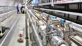
The programme included extensive reviews of the almost completed systems for the major LHC experiments – ALICE, ATLAS, CMS and LHCb. The talks and informal discussions showed the great progress there has been in commissioning these impressive systems with test beams and cosmic rays. As the experiments gear up for data-taking, the teams are validating and refining the tracking, alignment and vertex-reconstruction software tools. There are, however, concerns about exposing these detectors at frighteningly close distances to the beams in an accelerator that has not yet run. There were presentations of plans for experiment protection at the LHC, but the information provided did not quell the debate.
While everyone is eagerly awaiting data-taking at the LHC, there are already plans for upgrades and new facilities. The world community is poised to meet the challenges of vertex detectors for the proposed International Linear Collider, high-luminosity upgrades of the LHC – the Super LHC (SLHC) – and flavour physics experiments (a Super B-factory and an upgrade of the LHCb experiment). Many upgrade paths require vertex detectors with improved radiation hardness and higher segmentation to cope with the higher multiplicities and higher event rates. In addition, several considerations, not the least of which is the amount of material, motivate the effort towards detector thinning.
Upgraded experiments will also require upgraded analysis tools. Many important new particles, such as Higgs bosons, are likely to decay into B particles. These leave displaced vertices, so algorithms that provide this information, especially in the earlier stages of the trigger processor, will be necessary. This is a paramount consideration in the LHCb upgrade and provides a strong motivation to pursue a pixel-based vertex detector.
Novel devices
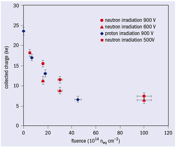
A strong focus of this workshop centred on the evaluation of new devices developed to address a variety of the challenges posed by future projects. Radiation hardness, for example, is a critical consideration for SLHC upgrades. This is the motivation behind RD50, a large R&D effort based at CERN that involves scientists from all over the world. After years of R&D on a variety of technologies and structures, this group is now reaching important conclusions. In particular, devices using “n+” electrodes (pixels or strips) implanted on p-type substrates appear to be one of the most effective options to cope with increased radiation fluence. Speakers presented recent results and showed that microstrip detectors can still be operated after being irradiated at fluencies up to 1016 neutrons/cm2, as required in the innermost layers at SLHC luminosities (figure 1). One plane of a strip-detector implemented on p-type substrates has been installed in LHCb, “the first full-scale SLHC silicon plane”. Although the traditional emphasis of this conference is on silicon-based technology, discussions also covered the naturally radiation-hard diamond detectors, in particular the promising single-crystal diamond devices.
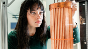
The reduced collection distance achievable at high levels of irradiation has helped to inspire renewed interest in thinned silicon. The workshop learned that this performs just as well as “thick” 300-μm detectors after sufficient radiation, as the charge cannot be collected out of the thicker sensors. In addition, examples were shown of detectors thinned down to 10 μm that are functional and mechanically stable. Other novel detector concepts included 3-dimensional detectors; monolithic devices, where the readout chip is made on the same silicon substrate as used for the sensor; and DEPFET, where each pixel is a p-channel FET on a completely depleted bulk. Another interesting development is the so-called “3D integration”, featuring integration of the sensor and several layers of readout electronics, which is facilitated by the strong push towards miniaturization in the computer industry.
Silicon micropattern detectors are central to precision imaging in several areas of research, from medicine to biology, to astrophysics and astroparticle physics. The field is in rapid evolution and several interesting talks highlighted a broad spectrum of applications. Examples of imaging geared towards medical or biological applications included the MEDIPIX chip, 3H imaging, NANO-CT scanning, and the PILATUS system – a pixelated hybrid silicon X-ray detector developed for protein crystallography at the Swiss Light Source. Astrophysics applications included PAMELA, now taking data in space, and the more futuristic EXIST, a proposed large-area telescope for X-ray astronomy.
• The next meeting in the series will be run by Richard Brenner and held near Stockholm in the summer.