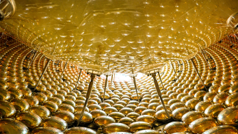
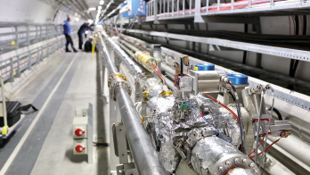
The EPS-TIG meeting looked at applications ranging from medicine to materials science.
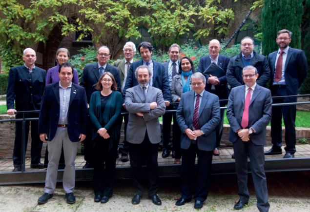
Image credit: Giampiero Corelli Fotoreporter, Ravenna.
The European Physical Society’s Technology and Innovation Group (EPS-TIG) was set up in 2011 to work at the boundary between basic and applied sciences, with annual workshops organized in collaboration with CERN as its main workhorse (CERN Courier April 2013 p31). The second workshop, organized in conjunction with the department of physics and astronomy and the “Fondazione Flaminia” of Bologna University, took place in Ravenna on 11–12 November 2013. The subject – advanced radiation detectors for industrial use – brought experts involved in the research and development of advanced sensors, together with representatives from related spin-off companies.
The first session, on technology-transfer topics, opened with a keynote speech by Karsten Buse, director of the Fraunhofer Institute for Physical Measurement Technique (IPM), Freiburg. In the spirit of Joseph von Fraunhofer (1787–1826) – a researcher, inventor and entrepreneur – the Fraunhofer Gesellschaft promotes innovation and applied research that is of direct use for industry. Outlining the IPM’s mission and the specific competences and services it provides, Buse presented an impressive overview of technology projects that have been initiated and developed or improved and supported by the institute. He also emphasized the need to build up and secure intellectual property, and explained contract matters. The success stories include the MP3 audio-compression algorithm, white LEDs to replace conventional light bulbs, and all-solid-state widely tunable lasers. Buse concluded by observing that bridging the gap between academia and industry requires some attention, but is less difficult than often thought and also highly rewarding. A lively discussion followed in the audience of students, researchers and partners from industry.
The second talk focused on knowledge transfer (KT) from the perspective of CERN’s KT Group. First, Giovanni Anelli described the KT activities based on CERN’s technology portfolio and on people – that is, students and fellows. In the second part, Manjit Dosanjh presented the organization’s successful and continued transfer to medical applications of advanced technologies in the fields of accelerators, detectors and informatics technologies. Catalysing and facilitating collaborations between medical doctors, physicists and engineers, CERN plays an important role in “physics for health” projects at the European level via conferences and networks such as ENLIGHT, set up to bring medical doctors and physics researchers together (CERN Courier December 2012 p19).
Andrea Vacchi of INFN/Trieste reviewed the INFN’s KT activities. He emphasized that awareness of the value of the technology assets developed inside INFN is growing. In the past, technology transfer between INFN and industry happened mostly through the involvement of suppliers in the development of technologies. In future, INFN will take more proactive measures to encourage technology transfer between INFN research institutions and industry.
From lab to industry
The first afternoon was rounded up by Colin Latimer of the University of Belfast and member of the EPS Executive Committee. He illustrated the varying timescales between invention and mass-application multi-billion-dollar markets, with a number of example technologies including optical fibres (1928), liquid-crystal displays (1936), magnetic-resonance imaging (MRI) scanners (1945) and lasers (1958), with high-temperature superconductors (1986) and graphene (2004) still waiting to make a major impact. Latimer went on to present results from the recent study commissioned by the EPS from the Centre for Economics and Business Research, which has shown the importance of physics to the European economy (EPS/Cebr 2013).
The second part of the workshop was devoted to sensors and innovation in instrumentation and industrial applications, starting with a series of talks that reviewed the latest developments. This was followed by presentations from industry on various sensor products, application markets and technological developments.
Erik Heijne, a pioneer of silicon and silicon-pixel detectors at CERN, started by discussing innovation in instrumentation through the use of microelectronics technology. Miniaturization to sub-micron silicon technologies allows many functions to be compacted into a small volume. This has led in turn to the integration of sensors and processing electronics in powerful devices, and has opened up new fields of applications (CERN Courier March 2014 p26). In high-energy particle physics, the new experiments at the LHC have been based on sophisticated chips that allow unprecedented event rates of up to 40 MHz. Some of the chips – or at least the underlying ideas – have found applications in materials analysis, medical imaging and other types of industrial equipment. The radiation imaging matrix, for example, based on silicon-pixel and integrated read-out chips, has many applications already.
Detector applications
Julia Jungmann of PSI emphasized the use of active pixel detectors for imaging in mass spectrometry in molecular pathology, in research done at the FOM Institute AMOLF in Amsterdam. The devices have promising features for fast, sensitive ion-imaging with time and space information from the same detector, high spatial resolution, direct imaging acquisition and highly parallel detection. The technique, which is based on the family of Medipix/Timepix devices, provides detailed information on molecular identity and localization – vital, for example in detecting the molecular basis of a pathology without the need to label bio-molecules. Applications include disease studies, drug-distribution studies and forensics. The wish list is now for chips with 100 ps time bins, a 1 ms measurement interval, multi-hit capabilities at the pixel level, higher read-out rates and high fluence tolerance.
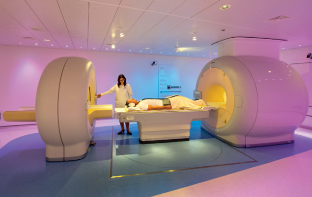
Image credit: Philips.
In a similar vein, Alberto Del Guerra of the University of Pisa presented the technique of positron-emission tomography (PET) and its applications. Outlining the physics and technology of PET, he showed improved variants of PET systems and applications to molecular imaging, which also allow the visual representation, characterization and quantification of biological processes at the cellular and subcellular levels within living organisms. Clinical systems of hybrid PET and computerized tomography (CT) for application in oncology and neurology, human PET and micro-PET equipment, combined with small-animal CT, are available from industry, and today there are also systems where PET and magnetic resonance imaging (MRI) are combined. Such systems are being used in hadron therapy in Italy for monitoring purposes at the 62 MeV proton cyclotron of the CATANA facility in Catania, and at the proton and carbon synchrotron of the CNAO centre in Pavia. An optimized tri-modality imaging tool for schizophrenia is even being developed, combining PET with MRI and electroencephalography measurements. Del Guerra’s take-home message was that technology transfer in the medical field needs long-term investment – industry can withdraw halfway if a technology is not profitable (for example, Siemens in the case of proton therapy). In future, applications will be multimodal with PET combined with other imaging techniques (CT, MRI, optical projection tomography), for applications to specific organs such as the brain, breast, prostate and more.
The next topic related to recent developments in the silicon drift detector (SDD) and its applications. Chiara Guazzoni, of the Politecnico di Milano and INFN Milan, gave an excellent overview of SDDs, which were invented by Emilio Gatti and Pavel Rehak 30 years ago. These detectors are now widely used in X-ray spectroscopy and are commercially available. Conventional and non-conventional applications include the non-destructive analysis of cultural heritage and biomedical imaging based on X-ray fluorescence, proton-induced X-ray emission studies, gamma-ray imaging and spectroscopy, X-ray scatter imaging, etc. As Gatti and Rehak stated in their first patent, “additional objects and advantages of the invention will become apparent to those skilled in the art,” and Guazzoni hopes that the art will keep “drifting on” towards new horizons.
Moving on to presentations from industry and start-up companies, Jürgen Knobloch of KETEK GmbH in Munich presented new high-throughput, large-area SDDs, starting with a historical review of the work of Josef Kemmer, who in 1970 started to develop planar silicon technology for semiconductor detectors. Collaborating with Rehak and the Max-Planck Institute in Munich, Kemmer went on to produce the first SDDs with a homogeneous entrance window, with depleted field-effect transistor (DEPFET) and MOS-type DEPFET (DEPMOS) technologies. In 1989 he founded the start-up company KETEK, which is now the global commercial market leader in SSD technology. Knobloch presented the range of products from KETEK and concluded with a list of recommendations for better collaboration between research and industry. KETEK’s view on how science and industry can better collaborate includes: workshops of the kind organized by EPS-TIG; meetings between scientists and technology companies to set out practical needs and future requirements; involvement of technology-transfer offices to resolve intellectual-property issues; encouragement of industry to accept longer times for returns in investments; and the strengthening of synergies between basic research and industry R&D.
Knobloch’s colleague at KETEK, Werner Hartinger, then described new silicon photomultipliers (SiPMs) with high proton-detection efficiency, and listed the characteristics of a series of KETEK’s SiPM sensors, which also feature a huge gain (> 106) with low excess noise and a low temperature coefficient. KETEK has off-the-shelf SiPM devices and also customizes devices for CERN. The next steps will be continuous noise reduction (in both dark rate and cross-talk) by enhancing the KETEK “trench” technology, enhancement of the pulse shape and timing properties by optimizing parasitic elements and read-out, and the production of chip-size packages and arrays at the package level.
New start-ups
PIXIRAD, a new X-ray imaging system based on chromatic photon-counting technology, was presented by Ronaldo Bellazzini of PIXIRAD Imaging Counters srl – a recently constituted INFN spin-off company. The detector can deliver extremely clear and highly detailed X-ray images for medical, biological, industrial and scientific applications in the energy range 1–100 keV. Photon counting, colour mode and high spatial resolution lead to an optimal ratio of image quality to absorbed dose. Modules with units of 1, 2, 4 and 8 tiles have been built with almost zero dead space between the blocks. A complete X-ray camera based on the PIXIRAD-1 single-module assembly is available for customers in scientific and industrial markets for X-ray diffraction, micro-CT, etc. A dedicated machine to perform X-ray slot-scanning imaging has been designed and built and is currently under test. This system, which uses the PIXIRAD-8 module and is able to produce large-area images with fine position resolution, has been designed for digital mammography, which is one of the most demanding X-ray imaging applications.
CIVIDEC Instrumentation – another start-up company – was founded in 2009 by Erich Griesmayer. He presented several examples of applications of the products, which are based on diamond-detector technology. They have found use at the LHC and other accelerator beamlines as beam-loss and beam-position monitors for time measurements, high-radiation-level measurements, neutron time of flight, and as low-temperature detectors in superconducting quadrupoles. The company provides turn-key solutions that connect via the internet, supplying clients worldwide.
Nicola Tartoni, head of the detector group at the Diamond Light Source, outlined the layout of the facility and its diversified programmes. He presented an overview of the detector development and beamlines of this outstanding user facility in partnership with industry, with diverse R&D projects of increasing complexity.
Last, Carlos Granja, of the Institute of Experimental and Applied Physics (IEAP) at the Czech Technical University (CTU) in Prague, described the research carried out with the European Space Agency (ESA) demonstrating the impressive development in detection and particle tracking of individual radiation quanta in space. This has used the Timepix hybrid semiconductor pixel-detector developed by the Medipix collaboration at CERN. The Timepix-based space-qualified payload, produced by IEAP CTU in collaboration with the CSRC company of the Czech Republic, has been operating continuously on board ESA’s Proba-V satellite in low-Earth orbit at 820 km altitude, since being launched in May 2013. Highly miniaturized devices produced by IEAP CTU are also flying on board the International Space Station for the University of Houston and NASA for high-sensitivity quantum dosimetry of the space-station crew.
In other work, IEAP CTU has developed a micro-tracker particle telescope in which particle tracking and directional sensitivity are enhanced by the stacked layers of the Timepix device. For improved and wide-application radiation imaging, edgeless Timepix sensors developed at VTT and Advacam in Finland, with advanced read-out instrumentation and micrometre-precision tiling technology (available at IEAP CTU and the WIDEPIX spin-off company, of the Czech Republic), enable large sensitive areas up to 14 cm square to be covered by up to 100 Timepix sensors. This development allows the extension of high-resolution X-ray and neutron imaging at the micrometre level to a range of scientific and industrial applications.
• For more about the workshop, visit www.emrg.it/TIG_Workshop_2013/program.php?language=en. For the presentations, see http://indico.cern.ch/event/284070/.


