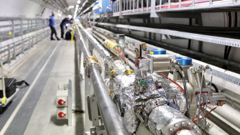
Pictures ultimately provide the most graphic record of of particle interactions. For CERN’s LHC collider, sophisticated electronic “eyes” at the heart of the big ATLAS and CMS detectors will pick up the tracks left by the particles fleeing from the collisions and search for masterpieces to hang in the next century’s gallery of research art.
Whatever means are used to record the result of high-energy collisions, it is still important for physicists to have “pictures” of the tracks left by the emerging particles. In middle of the century, these tracks were captured photographically in mechanically operated cloud and bubble chambers, whose annals provided a dramatic photo album of physics progress. These chambers have been superseded by sophisticated electronic detectors in which the particles produce signals in successive layers of sensors surrounding the particle collision site. A computer-driven pattern recognition system disentangles a cloud of discrete points, joining together related signals to reveal the tracks and provide an electronic snapshot of the collision. For CERN’s LHC collider, it is the inner tracking systems of the big ATLAS and CMS detectors that will illustrate the research albums for the beginning of the 21st century.
The Technical Design Reports for the ATLAS pixel detector and CMS Tracker have now been formally approved and become subject to stringent scheduling and monitoring to ensure commissioning in the year 2005.
ATLAS pixels
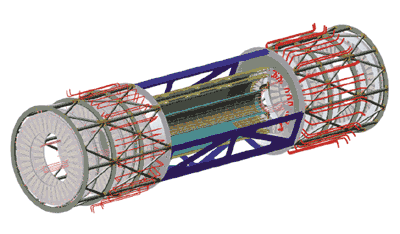
The heart of the mighty ATLAS detector being constructed for CERN’s LHC proton collider will record the sprays of particles emerging directly from particle collisions at energies never before explored. This core “vertex detector”, a direct descendant of the old bubble chamber, will track the fine central lacework of these complicated processes. These innermost signals will be vital for the subsequent layers of detector to follow the particles emerging from each LHC interaction.
The technique being used is semiconductor pixels, a technology pioneered at fixed-target experiments and previously used in vertex detectors at the Delphi and SLD experiments respectively at CERN’s LEP and Stanford’s SLC electronpositron colliders. Pixels tiny diodes implanted on semiconductor wafers pick up the ionization produced by charged particles and offer high spatial resolution in two directions, fixing where particles have passed to within ten microns.
ATLAS pixels will be arranged in three layers in a central barrel of 80 cm length immediately around the collision point, supplemented by five discs either side in the beam direction. The barrel sensors will overlap to ensure that there are no cracks through which particles can escape undetected. The key innermost barrel layer (radius 4 cm) will use 200 micron sensors, while the remainder will use 250 micron thickness. Together with their readout electronics, these will form 1508 barrel modules and 720 disk modules. Although mounted on different structures, the barrel and disk sensors are the same.
Particle bombardment
Using pixels for ATLAS brings new challenges. Firstly, the semiconductors will have to be able to withstand the intense particle bombardment close to the interaction point, with several collisions every 25 nanoseconds each producing hundreds of secondary particles. This could easily spoil the semiconductor properties of the detectors.
Secondly, pixel readout has always needed sophisticated electronics, but in this case the problem is exacerbated by the torrent of data emerging, equivalent to about 100 Megabytes per second.
Thirdly, the substrate of each semiconductor element has to be reliably fixed (bump-bonded) to its support and connections, and finally the array of pixels has to be mechanically supported without interfering too much with the emerging particles, and with adequate cooling. All this for about a hundred million pixels.
The baseline sensor choice is n+ implants on n-type substrate, with individual sensors isolated either via high-dose p-implant surrounds, or by spraying the whole n-surface with medium dose p-implant which is overcompensated by the high dose pixel implants of the sensors themselves. Both techniques show encouraging results and both are being pursued prior to making a final design decision. 4 inch wafers containing two sensor tiles have been fabricated by industry in Germany and in Japan, using both types of isolation in each wafer.
Readout electronics
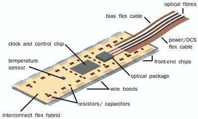
Readout electronics is a real challenge. With highly irradiated sensors and thin layers, pixel front-end electronics will have to cope with very small signals. In addition, readout of the few thousand pixels hit during a bunch crossing requires sophisticated architecture with lots of task parallelism and data compression. All the electronics has to be built using radiation-hard components, however, initial design and prototyping will be accelerated by using rad-soft electronics. Data is transmitted via optical fibres.
For the integration of sensors and electronics, bump bonding using indium and solder are both being evaluated using test beams at CERN, with a microstrip telescope fixing tracks to 5 microns.
For the mechanical support, a key element is the thermal management tile (TMT), each one of which has to support 13 modules and drain off about 15 kW of heat produced by 2 m2 of integrated electronics. This is done via a cooling tube, supported by an omega-shaped backbone framework. Sensors have to be maintained at 6 °C. Several TMT solutions are being investigated.
Having taken the plunge to go for semiconductor pixels, initial tests are progressing well. Several design decision still remain, but the heart of the ATLAS detector is on schedule to begin pumping for the first LHC collisions in 2005.
Information from Leonardo Rossi, Genoa.