First developed for the Large Hadron Collider, hybrid pixel detectors are now changing the face of X-ray imaging in medical practice. The next challenge is for a diverse range of societal applications to exploit precise timing at the pixel level, say Rafael Ballabriga, Michael Campbell and Xavier Llopart.
In 1885, in a darkened lab in Würzburg, Bavaria, Wilhelm Röntgen noticed that a screen coated with barium platinocyanide fluoresced, despite being shielded from the electron beam of his cathode-ray tube. Hitherto undiscovered “X”-rays were being emitted as the electrons braked sharply in the tube’s anode and glass casing. A week later, Röntgen imaged his wife’s hand using a photographic plate, and medicine was changed forever. X-rays would be used for non-invasive diagnosis and treatment, and would inspire countless innovations in medical imaging. Röntgen declined to patent the discovery of X-ray imaging, believing that scientific advancements should benefit all of humanity, and donated the proceeds of the first Nobel Prize for Physics to his university.
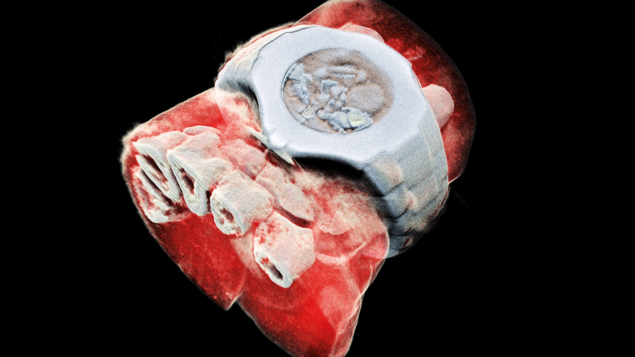
One hundred years later, medical imaging would once again be disrupted – not in a darkened lab in Bavaria, but in the heart of the Large Hadron Collider (LHC) at CERN. The innovation in question is the hybrid pixel detector, which allows remarkably clean track reconstruction. When the technology is adapted for use in a medical context, by modifying the electronics at the pixel level, X-rays can be individually detected and their energy measured, leading to spectroscopic X-ray images that distinguish between different materials in the body. In this way, black and white medical imaging is being reinvented in full colour, allowing more precise diagnoses with lower radiation doses.
The next step is to exploit precise timing in each pixel. The benefits will be broadly felt. Electron microscopy of biological samples can be clearer and more detailed. Biomolecules can be more precisely identified and quantified by imaging time-of-flight mass spectrometry. Radiation doses can be better controlled in hadron therapy, reducing damage to healthy tissue. Ultra-fast changes can be captured in detail at synchrotron light sources. Hybrid pixel detectors with fast time readout are even being used to monitor quantum-mechanical processes.
Digital-camera drawbacks
X-ray imaging has come a long way since the photographic plate. Most often, the electronics work in the same way as a cell-phone camera. A scintillating material converts X-rays into visible photons that are detected by light-sensitive diodes connected to charge-integrating electronics. The charge from high-energy and low-energy photons is simply added up within the pixel in the same way a photographic film is darkened by X-rays.

Charge integration is the technique of choice in the flat-panel detectors used in radiology as large surfaces can be covered relatively cheaply, but there are several drawbacks. It’s difficult to collect the scintillation light from an X-ray on a single pixel, as it spreads out. And information about the energy of the X-rays is lost.
By the 1990s, however, LHC detector R&D was driving the development of the hybrid pixel detector, which could solve both problems by detecting individual photons. It soon became clear that “photon counting” could be as useful in a hospital ward as it would prove to be in a high-energy-physics particle detector. In 1997 the Medipix collaboration first paired semiconductor sensors with readout chips capable of counting individual X-rays.
Nearly three decades later, hybrid pixel detectors are making their mark in hospital wards. Parallel to the meticulous process of preparing a technology for medical applications in partnership with industry, researchers have continued to push the limits of the technology, in pursuit of new innovations and applications.
Photon counting
In a hybrid pixel detector, semiconductor sensor pixels are individually fixed to readout chips by an array of bump bonds – tiny balls of solder that permit the charge signal in each sensor pixel to be passed to each readout pixel (see “Hybrid pixels” figure). In these detectors, low-noise pulse-processing electronics take advantage of the intrinsic properties of semiconductors to provide clean track reconstruction even at high rates (see “Semiconductor subtlety” panel).
Since silicon detectors are relatively transparent to the X-ray energies used in medical imaging (approximately 20 to 140 keV), denser sensor materials with higher stopping power are required to capture every photon passing through the patient. This is where hybrid pixel detectors really come into their own. For X-ray photons with an energy above about 20 keV, a highly absorbing material such as cadmium telluride can be used in place of the silicon used in the LHC experiments. Provided precautions are taken to deal with charge sharing between pixels, the number of X-rays in every energy bin can be recorded, allowing each pixel to measure the spectrum of the interacting X-rays.
Semiconductor subtlety
In insulators, the conduction band is far above the energy of electrons in the valence band, making it difficult for current to flow. In conductors, the two bands overlap and current flows with little resistance. In semiconductors, the gap is a just a couple of electron-volts. Passing charged particles, such as those created in the LHC experiments, promotes thousands of valence electrons into the conduction band, creating positively charged “holes” in the valence band, allowing current to flow.
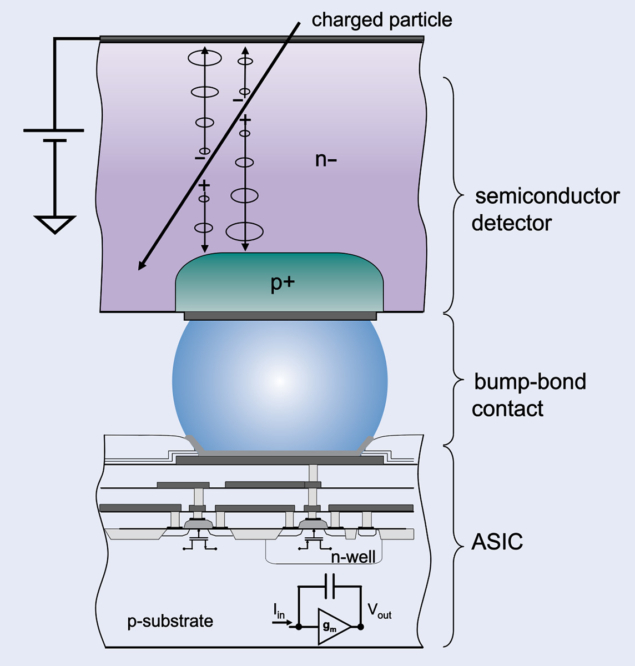
Silicon has four valence electrons and therefore forms four covalent bonds with neighbouring atoms to fill up its outermost shell in silicon crystals. These crystals can be doped with impurities that either add additional electrons to the conduction band (n-type doping) or additional holes to the valence band (p-type doping). The silicon pixel sensors used at the LHC are made up of rectangular pixels doped with additional holes on one side coupled to a single large electrode doped with additional electrons on the rear (see “Pixel picture” figure).
In p-n junctions such as these, “depletion zones” develop at the pixel boundaries, where neighbouring electrons and holes recombine, generating a natural electric field. The depletion zones can be extended throughout the whole sensor by applying a strong “reverse-bias” field in the opposite direction. When a charged particle passes, electrons and holes are created as before, but thanks to the field a directed pulse of charge now flows across the bump bond into the readout chip. Charge collection is prompt, permitting the pixel to be ready for the next particle.
In each readout pixel the detected charge pulse is compared with an externally adjustable threshold. If the pulse exceeds the threshold, its amplitude and timing can be measured. The threshold level is typically set to be many times higher than the electronic noise of the detection circuit, permitting noise-free images. Because of the intimate contact between the sensor and the readout circuit, the noise is typically less than a root-mean-square value of 100 electrons, and any signal higher than a threshold of about 500 electrons can be unambiguously detected. Pixels that are not hit remain silent.
In the LHC, each passing particle liberates thousands of electrons, allowing clean images of the collisions to be taken even at very high rates. Hybrid pixels have therefore become the detector of choice in many large experiments where fast and clean images are needed, and are the heart of the ATLAS, CMS and LHCb experiments. In cases where the event rates are lower, such as the ALICE experiment at the LHC and the Belle II experiment at SuperKEKB at KEK in Japan, it has now become possible to use “monolithic” active pixel detectors, where the sensor and readout electronics are implemented in the same substrate. In the future, as the semiconductor industry shifts to three-dimensional chip and wafer stacking, the distinction between hybrid and monolithic pixel detectors will be blurred.
Protocols regarding the treatment of patients are strictly regulated in the interest of safety, making it challenging to introduce new technologies. Therefore, in parallel with the development of successive generations of Medipix readout chips, a workshop series on the medical applications of spectroscopic X-ray detectors has been hosted at CERN. Now in its seventh edition (see “Threshold moment for medical photon counting”), the workshop gathers representatives of cross-disciplinary specialists ranging from the designers of readout chips to specialists in the large equipment suppliers, and from medical physicists all the way up to opinion-leading radiologists. The role of the workshop is the formation and development of a community of practitioners from diverse fields willing to share knowledge – and, of course, reasonable doubts – in order to encourage the transition of spectroscopic photon counting from the lab to the clinic. CERN and the Medipix collaborations have played a pathfinding role in this community, exploring avenues well in advance of their introduction to medical practice.
The Medipix2 (1999–present), Medipix3 (2005–present) and Medipix4 (2016–present) collaborations are composed only of publicly funded research institutes and universities, which helps keep the development programmes driven by science. There have been hundreds of peer-reviewed publications and dozens of PhD theses written by the designers and users of the various chips. With the help of CERN’s Knowledge Transfer Office, several start-up companies have been created and commercial licences signed. This has led to many unforeseen applications and helped enormously with the dissemination of the technology. The publications of the clients of the industrial partners now represent a large share of the scientific outcome from these efforts, totalling hundreds of papers.
Spectroscopic X-ray imaging is now arriving in clinical practice. Siemens Healthineers were first to market in 2022 with the Naeotom Alpha photon counting CT scanner, and many of the first users have been making ground-breaking studies exploiting the newly available spectroscopic information in the clinical domain. CERN’s Medipix3 chip is at the heart of the MARS Bioimaging scanner, which brings unprecedented imaging performance to the point of patient care, opening up new patient pathways and saving time and money.
ASIC (application-specific integrated circuit) development is still moving forwards rapidly in the Medipix collaborations. For example, in the Medipix3 and Medipix4 chips, on-pixel circuitry mitigates the impact of X-ray fluorescence and charge diffusion in the semiconductor by summing up the charge in a localised region and allocating the hit to one pixel. The fine segmentation of the detector not only leads to unprecedented spatial resolution but also mitigates “hole trapping” – a common bugbear of the high-density sensor materials used in medical imaging, whereby photons of the same energy induce different charges according to their interaction depth in the sensor. Where the pixel size is significantly smaller than the perpendicular sensor thickness – as in the Medipix case – only one of the charge species (usually electrons) contributes to the measured charge, and no matter where the X-ray is deposited in the sensor thickness, the total charge detected is the same.
But photon counting is only half the story. Another parameter that has not yet been exploited in high-spatial-resolution medical imaging systems can also be measured at the pixel level.
A new dimension
In 2005, Dutch physicists working with gas detectors requested a modification that would permit each pixel to measure arrival times instead of counting photons. The Medipix2 collaboration agreed and designed a chip with three acquisition modes: photon counting, arrival time and time over threshold, which provides a measure of energy. The Timepix family of pixel-detector readout chips was born.

The most recent generations of Timepix chips, such as Timepix3 (released in 2016) and Timepix4 (released in 2022) stream hit information off chip as soon as it is generated – a significant departure from Medipix chips, which process hits locally, assuming them to be photons, sending only a spectroscopic image off chip. With Timepix, each time a charge exceeds the threshold, a packet of information is sent off chip that contains the coordinates of the hit pixel, the particle’s arrival time and the time over threshold (66 bits in total per hit). This allows offline reconstruction of individual clusters of hits, opening up a myriad of potential new applications.
One advantage of Timepix is that particle event reconstruction is not limited to photons. Cosmic muons leave a straight track. Low-energy X-rays interact in a point-like fashion, lighting up only a small number of pixels. Electrons interact with atomic electrons in the sensor material, leaving a curly track. Alpha particles deposit a large quantity of charge in a characteristic blob. To spark the imagination of young people, Timepix chips have been incorporated on a USB thumb drive that can be read out on a laptop computer (see “Thumb-drive detector” figure). The CERN & Society Foundation is raising funds to make these devices widely available in schools.
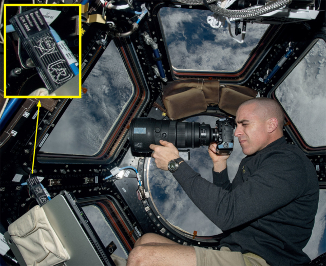
Timepix chips have also been adapted to dose monitoring for astronauts. Following a calibration effort by the University of Houston, NASA and the Institute for Experimental and Applied Physics in Prague, a USB device identical to that used in classrooms precisely measures the doses experienced by flight crews in space. Timepix is now deployed on the International Space Station (see “Radiation monitoring” figure), the Artemis programme and several European space-weather studies, and will be deployed on the Lunar Gateway programme.
Stimulating innovation
Applications in science, industry and medicine are too numerous to mention in detail. In time-of-flight mass spectrometry, the vast number of channels allowed by Timepix promises new insights into biomolecules. Large-area time-resolved X-ray cameras are valuable at synchrotrons, where they have applications in structural biology, materials science, chemistry and environmental science. In the aerospace, manufacturing and construction industries, non-destructive X-ray testing using backscattering can probe the integrity of materials and structures while requiring access from one side only. Timepix chips also play a crucial role in X-ray diffraction for materials analysis and medical applications such as single-photon-emission computed tomography (SPECT), and beam tracking and dose-deposition monitoring in hadron therapy (see “Carbon therapy” figure). The introduction of noise-free hit streaming with timestamp precision down to 200 picoseconds has also opened up entirely new possibilities in quantum science, and early applications of Timepix3 in experiments exploring the quantum behaviour of particles are already being reported. We are just beginning to uncover the potential of these innovations.
It’s also important to note that applications of the Timepix chips are not limited to the readout of semiconductor pixels made of silicon or cadmium telluride. A defining feature of hybrid pixel detectors is that the same readout chip can be used with a variety of sensor materials and structures. In cases where visible photons are to be detected, an electron can be generated in a photocathode and then amplified using a micro-channel plate. The charge cloud from the micro-channel plate is then detected on a bare readout chip in much the same way as the charge cloud in a semiconductor sensor. Some gas-filled detectors are constructed using gas electron multipliers and micromegas foils, which amplify charge passing through holes in the foils. Timepix chips can be used for readout in place of the conventional pad arrays, providing much higher spatial and time resolution than would otherwise be available.
Successive generations of Timepix and Medipix chips have followed Moore’s law, permitting more and more circuitry to be fitted into a single pixel as the minimum feature size of transistors has shrunk. In the Timepix3 and Timepix4 chips, data-driven architecture and on-pixel time stamping are the unique features. The digital circuitry of the pixel has become so complex that an entirely new approach to chip design – “digital-on-top” – was employed. These techniques were subsequently deployed in ASIC developments for the LHC upgrades.
Just as hybrid-pixel R&D at the LHC has benefitted societal applications, R&D for these applications now benefits fundamental research. Making highly optimised chips available to industry “off the shelf” can also save substantial time and effort in many applications in fundamental research, and the highly integrated R&D model whereby detector designers keep one foot in both camps generates creativity and the reciprocal sparking of ideas and sharing of expertise. Timepix3 is used as readout of the beam–gas-interaction monitors at CERN’s Proton Synchrotron and Super Proton Synchrotron, providing non-destructive images of the beams in real time for the first time. The chips are also deployed in the ATLAS and MoEDAL experiments at the LHC, and in numerous small-scale experiments, and Timepix3 know-how helped develop the VeloPix chip used in the upgraded tracking system for the LHCb experiment. Timepix4 R&D is now being applied to the development of a new generation of readout chips for future use at CERN, in applications where a time bin of 50 ps or less is desired.
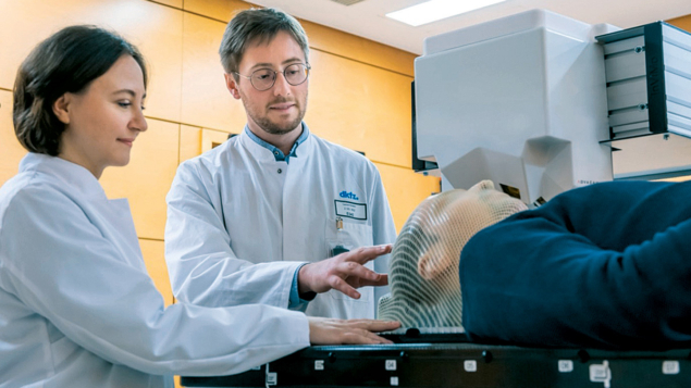
All these developments have relied on collaborating research organisations being willing to pool the resources needed to take strides into unexplored territory. The effort has been based on the solid technical and administrative infrastructure provided by CERN’s experimental physics department and its knowledge transfer, finance and procurement groups, and many applications have been made possible by hardware provided by the innovative companies that license the Medipix and Timepix chips.
With each new generation of chips, we have pushed the boundaries of what is possible by taking calculated risks ahead of industry. But the high-energy-physics community is under intense pressure, with overstretched resources. Can blue-sky R&D such as this be justified? We believe, in the spirit of Röntgen before us, that we have a duty to make our advancements available to a larger community than our own. Experience shows that when we collaborate across scientific disciplines and with the best in industry, the fruits lead directly back into advancements in our own community.


