3D silicon detectors offer exciting new approaches to imaging for particle physics and other fields. Cinzia DaVia’ explains.
Silicon is the material of choice for the tracking detectors being made for experiments at CERN’s Large Hadron Collider (LHC). Silicon offers reliable, fast and cheap detectors. Segmented detectors, processed using microelectronic planar technology, have been used successfully to precisely image the tracks of charged particles in many experiments. The operation of such devices, however, is compromised when they are irradiated with high fluences (above 5 ¥ 1014 particles/cm2) of neutrons or high-energy hadrons, corresponding to about 5 years of LHC operation at a luminosity of 1034 cm-2 s-1 for detectors closest to the beam. Radiation-induced defects are introduced into the crystal lattice, completely transforming its electrical properties. A dramatic result of these changes is the loss of charge released by a traversing particle, produced for example by a proton-proton interaction in the LHC. This loss of information compromises the reconstruction of important events like the secondary vertices that would be produced by the decay of Higgs bosons into b quarks and antiquarks. Studies by a number of CERN-based research and development collaborations carried out in the past 10 years have helped physicists to understand and reduce radiation damage effects in silicon. The fundamental results obtained by these collaborations have contributed much to approximately doubling the useful life of trackers in the LHC’s ATLAS, CMS, ALICE and LHCb experiments to almost 10 years of operation.
An order-of-magnitude increase of the luminosity after the initial phase of the LHC experiments is the natural next step to improve the statistics for rare events. This would involve a reduction of the proton-proton bunch crossing to 12.5 ns, and an increase of beam intensity producing a consequent increase of the radiation rate (Gianotti et al. 2002). A new form of silicon sensor whose fabrication makes use of micromachining technology as well as the standard processes of planar technology, used for many years both for sensors and their readout chips, can satisfy these severe requirements.
3D solution
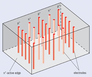
3D sensors proposed by Sherwood Parker of the University of Hawaii and colleagues in 1995 (figure 1), initially to solve the problem of charge loss in gallium arsenide detectors, have been fabricated using silicon (Parker et al. 1997). Active-edge 3D sensors, proposed in 1997 and also indicated in figure 1, should have efficient charge collection to within a few microns of their physical edges (Kenney et al. 2001). In this new configuration, the p+ and n+ electrodes penetrate through the silicon bulk, rather than being limited to the silicon wafer surface.
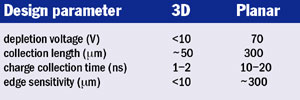
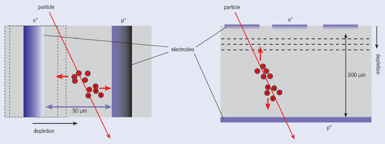
The advantages of 3D design, compared with the traditional planar design, are shown schematically in figure 2. Since the electric field is parallel (rather than orthogonal) to the detector surface, the charge collection distance can be several times shorter, the collection time considerably faster, and the voltage needed to extend the electric field throughout the volume between the electrodes (full depletion) an order of magnitude smaller, for 300 mm thick silicon (table 1).
This technology has many potential applications, for example in extreme radiation environments, luminosity monitors, and medical and biological imaging (Kenney et al. 2001, Parker et al. 2001).
Radiation effects in silicon detectors
Insulating layers on the surface of detectors charge up when traversed by charged particles. This can be tolerated. Damage to the bulk by both charged and neutral particles, however, is more difficult to combat. It takes just 25 eV to knock a silicon atom out of its lattice point. This leads to the formation of defects, in some instances involving impurity atoms in the material. Defects can be electrically active, leading to increased space-charge, leakage current and charge trapping. Increased space-charge prevents the electric field from penetrating the material unless high bias voltages are used. Moreover, radiation-induced space-charge can increase after the radiation source is removed, a phenomenon called reverse annealing. It has proven necessary to cool between -10°C and -20°C to reduce the leakage current and reverse annealing. The addition of oxygen into wafers has been found to reduce the space-charge build-up and improve reverse annealing for damage caused by charged particles. The use of multiguard structures, where biased guard rings surround the active detector area, has allowed high-voltage operation at the expense of larger inactive regions at the detector edge. Guard structures are used for achieving long-term stability, to reduce the current in the active area, and to prevent avalanche breakdown when high bias voltage is required. Cooling below 200 K also reduces the radiation-induced space-charge, which aids detector operation – a phenomenon called the Lazarus effect (Palmieri et al. 1998).
The electric field inside a silicon detector must be as large as possible
The electric field inside a silicon detector must be as large as possible. The risk of trapping of the carriers decreases if the electric field is large (figure 3). The effective drift length of a carrier (Ldrift = vdrift ¥ ttr) depends on the electric field value via the drift velocity vdrift. ttr is the trapping time of the carriers (the time taken by an electron or a hole to travel towards the collecting electrode before being trapped by a defect). It is clear that electrons will make a greater contribution to the signal, since their drift length is three times longer than that of holes. Drift lengths decrease linearly with fluence, making devices with a large collection distance inefficient at high radiation levels (DaVia’ and Watts 2002).
Prior to irradiation, electrons and holes contribute equally to the signal in the case of a pad detector where both electrodes have the same area. For a detector with a segmented collecting electrode, the larger fraction of the signal is produced by the carrier that travels towards it. This can be derived using a famous theorem due to Simon Ramo and (independently) William Shockley (Ramo 1939; Shockley 1938). Since electrons are harder to trap, it is important that the amplifier is connected to the n+ electrode, which collects electrons in a segmented detector. This is true for the ATLAS and CMS pixel detectors.

An example of the current state of the art is well illustrated by the pixel layers of the ATLAS vertex detector, which will be placed as close as 4 cm from the interaction point. The signal is collected on the n+ side of the detector. The n+ on n design is feasible by “spraying” a thin, moderately doped p layer between the n+ contacts, to prevent them from being shorted by electrons attracted to trapped positive charge at the interface between the field oxide and the silicon. The active thickness of the detector is reduced from the standard 300 mm to an average of around 230 mm to enhance the penetration of the electric field in the active area. This thickness, together with multiguard structure, allows operation up to around 600 V bias. This is a field of about 3 V/mm. Oxygenation of the wafer prior to detector processing reduces the radiation-induced space-charge, and consequently allows the detector to be fully depleted even after a fluence of 1015 particles/cm2. Under such conditions, about 98% of the signal charge generated in the detector is collected.
This result demonstrates that a combination of oxygenation and electron collection leads to efficient operation at reasonable bias voltages. This is important for power dissipation and thermal runaway, and has been further demonstrated by recent results from a group at Liverpool University, where similar conclusions were reached using a p-type silicon substrate (Casse et al. 2002).
3D detectors

Deep reactive ion etching has been developed for micromechanical systems. This allows microholes to be etched in silicon with a thickness-to-diameter ratio as large as 20:1. In the 3D detectors presently processed at Stanford, US, by a collaboration involving scientists from Brunel University in the UK, as well as Hawaii and Stanford, this technique is used to etch holes as deep as several hundred microns, at distances as short as 50 mm from one another. These holes are then filled with polycrystalline silicon doped with either boron or phosphorus, which is then diffused into the surrounding single-crystal silicon to make the detector electrodes (figure 4). The silicon substrate used for this process is p-type, and the crystal orientation is <100>, where 1,0,0 represent the crystal plane co-ordinates. Silicon atoms line up in certain directions in the crystal. <100> corresponds to having a particular crystal plane at the surface, and is preferred for a better surface quality. Once the electrodes are filled, the polycrystalline silicon is removed from the surfaces, and the dopant is diffused. Aluminium can be deposited in a pattern that will depend on how the individual electrodes are to be read out.
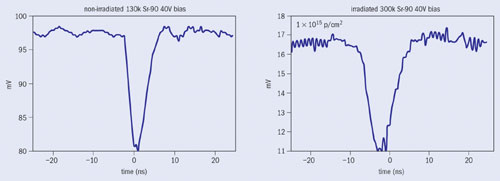
The response of a 3D detector, where all the electrodes have been connected together by an aluminium microstrip, is shown in the oscilloscope traces of figure 5. The fast radiation hard electronics used for this test were designed by the CERN microelectronics group (Anelli et al. 2002). The fast response, observed after 1015 protons/cm2 at room temperature and 40V bias voltage, confirms that the combination of short collection distance and high electric field can improve the radiation tolerance of silicon detectors by possibly a factor of 10 compared with planar devices. Improvement factors from better materials should multiply this geometric factor.
Active edges
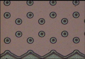
An example of a 3D sensor in the process of fabrication is shown in figure 6. The electrodes in this case are distributed in a hexagonal pattern, and the edges are completed by an active trench, doped appropriately to set the electric field distribution inside the detector. In planar devices, the conducting cut edge of the sensor must be prevented from shorting the bias voltage between the two surfaces by spacing the top and/or bottom of the electrodes away from the edges. Guard rings along the edges may also be added to intercept edge leakage current, and to drop the voltage in a controlled way. The resulting dead region at the edge will be at least comparable to the thickness and can be three or four times as large, so a space must be allowed for a series of guard rings.
In 3D devices, the voltage at corresponding points on the top and bottom surfaces is equal, so there is no voltage drop across the edges. Etched trenches, filled with suitably doped polycrystalline silicon, can then be used to make the edge into an electrode, with depletion possible to within a few microns of the physical edges. The freedom of such detectors from insensitive edge regions can be of great advantage when several devices are combined to cover large areas, or when the detector needs to be placed very close to the beam.
Silicon detectors are a good example to demonstrate how the particle physics community can benefit from the technology developed by the microelectronics industry. 3D geometry and active edges would have been an impossible dream only 10 years ago, and now they provide a natural way to construct imagers for charged particles and X-rays. The structural molecular biology community will take advantage of 3D detectors to study protein folding, while research is ongoing to apply this technology to X-ray mammography. Other groups are exploring alternative methods for fabricating 3D structures (Pellegrini et al. 2002).
Further reading
G Anelli et al. 2002 A high speed low noise transimpedence amplifier in a 0.25 mm CMOS technology, presented at ELMAU 2002, accepted for publication in Nucl. Instr. Meth. A.
G Casse et al. 2002 Nucl. Instr. Meth. A 487 465.
C DaVia’ and S J Watts 2002 Can silicon operate beyond 1015n/cm2?, presented at VERTEX 2001, accepted for publication in Nucl. Instr. Meth. A.
F Gianotti et al. 2002 Physics potential and experimental challenges of the LHC luminosity upgrade CERN-TH/2002-078 hep-ph/0204087.
C J Kenney et al. 2001 IEEE Trans. on Nucl. Sci. 48 (2) 189.
C Kenney, S Parker and E Walckiers 2001 IEEE Trans. on Nucl. Sci. 48 (6) 2405.
V G Palmieri et al. 1998 Nucl. Instr. Meth. A 413 475.
S I Parker, C J Kenney and J Segal 1997 Nucl. Instr. Meth. A 395 328.
S I Parker and C J Kenney 2001 IEEE Trans. on Nucl. Sci. 48 (5) 1629.
G Pellegrini et al. 2002 Nucl. Instr. Meth. A 487 19.
S Ramo 1939 Proc. IRE 27 584.
W Shockley 1938 J. Appl. Phys. 9 635.
3D detectors for physics and molecular biology applications: http://www.brunel.ac.uk/research/rose/3D.
ROSE collaboration: http://www.cern.ch/rd48.


