As an observer state of CERN, India is collaborating in many aspects of the Large Hadron Collider (LHC) project – building components of the accelerator as well as constructing detectors for various experiments. In the ALICE experiment, India is participating in the forward di-muon spectrometer (FMS) and in particular has responsibility for the design, fabrication and supply of the custom VLSI chip required for the spectrometer’s front-end electronics.
ALICE will study lead ion collisions at the LHC, where the production of the heavy quarkonia, such as the upsilon and its excited states, is expected to be suppressed. This is regarded as one of the strongest signals for the formation of a quark-gluon plasma.

Here, the yields of the upsilons will be measured by detecting their decays to two muons and determining the momenta of the muons though their bending in the field of a dipole magnet. The upsilon resonances will show up as “peaks” in the reconstructed invariant mass spectrum over a background of various other sources.
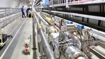
The tracks of the muons through the magnetic field will be measured in the FMS by a set of multiwire proportional chambers with finely segmented cathode pads. Muons passing through the detectors will produce signals on these pads, and their tracks will be reconstructed from a measurement by the front-end electronics of the charges deposited on the pads. Because of the high packing density and low noise required of the electronics readout, it is essential that the front-end electronics is realized in form of a custom-designed VLSI chip – the MANAS (Multiple Analog Signal processor).
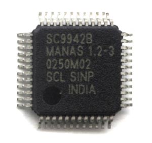
The design of the MANAS chip, based on the GASSIPLEX chip developed by Jean Claude Santiard at CERN, started in late 1997 at the Saha Institute of Nuclear Physics (SINP), Kolkata, and a memorandum of understanding was signed between SINP and Semiconductor Complex Ltd (SCL), Chandigarh, for the fabrication of the chip. Inside this chip, the signal from the detector is amplified by a charge-sensitive amplifier, processed by a deconvolution filter and shaping amplifier, tracked and stored, then finally read out via a multiplexer.
The final set of masks for fabrication of the MANAS-1.2-1 prototype was released by Bikash Sinha, SINP, in October 1999 and the first prototype ceramic packaged chips were delivered by SCL in March 2000. Extensive bench tests at SINP and CERN on the prototype chips were performed, followed by a beam test of the chip, mounted on a prototype detector for the second of the tracking stations (developed and fabricated at SINP) and exposed to a 7 GeV proton beam.
The results of these bench tests showed that the first prototype satisfied most of the design criteria. Two modified iterations of the design then corrected the problems found in the first prototype.
By January 2002, 1500 pre-production chips, MANAS-1.2-3, were sent to several institutes collaborating in the ALICE FMS for more extensive tests, both in the lab and in test beams. The main features of this state-of-the-art chip are the low noise level (640 electrons rms), small gain fluctuations, large dynamic range (500 to -275 fC), radiation tolerance and the low sensitivity of parameters to temperature variations.
The production readiness review for the MANAS chip was held in October 2003, and was based on results from various laboratories. More than 100 000 chips will be delivered by January 2005, after stringent quality and performance tests by the foundry, SCL in Chandigarh.
The MANAS chip is a definite success story for R&D and fabrication for high-technology VLSI development in India. It has already initiated more R&D activity in VLSI technology in India, and a large number of useful applications are being planned, including accurate image processing.