The recently installed, upgraded ALICE inner tracking system is the largest pixel detector ever built and the first at the LHC to use monolithic active pixel sensors, describe Luciano Musa and Stefania Beole.
In the coming decade, the study of nucleus–nucleus, proton–nucleus and proton–proton collisions at the LHC will offer rich opportunities for a deeper exploration of the quark–gluon plasma (QGP). An expected 10-fold increase in the number of lead–lead (Pb–Pb) collisions should both increase the precision of measurements of known probes of the QGP medium as well as give access to new ones. By focusing on rare probes down to very low transverse momentum, such as heavy-flavour particles, quarkonium states, real and virtual photons, as well the study of jet quenching and exotic heavy nuclear states, very large data samples will be required.
To seize these opportunities, the ALICE collaboration has undertaken a major upgrade of its detectors to increase the event readout, online data processing and recording capabilities by nearly two orders of magnitude (CERN Courier January/February 2019 p25). This will allow Pb–Pb minimum-bias events to be recorded at rates in excess of 50 kHz, which is the expected Pb–Pb interaction rate at the LHC in Run 3, as well as proton–lead (p–Pb) and proton–proton (pp) collisions at rates of about 500 kHz and 1 MHz, respectively. In addition, the upgrade will improve the ability of the ALICE detector to distinguish secondary vertices of particle decays from the interaction vertex and to track very low transverse-momentum particles, allowing measurements of heavy-flavour hadrons and low-mass dileptons with unprecedented precision and down to zero transverse momentum.
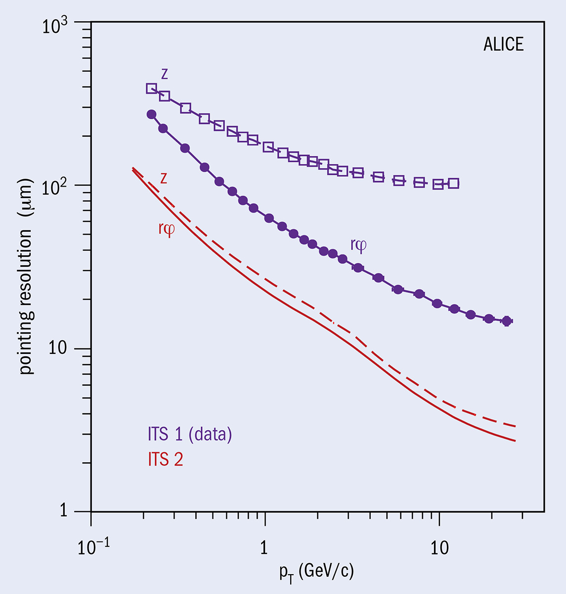
These ambitious physics goals have motivated the development of an entirely new inner tracking system, ITS2. Starting from LHC Run 3 next year, the ITS2 will allow pp and Pb–Pb collisions to be read out 100 and 1000 times more quickly than was possible in previous runs, offering superior ability to measure particles at low transverse momenta (see “High impact” figure). Moreover, the inner three layers of the ITS2 feature a material budget three times lower than the original detector, which is also important for improving the tracking performance at low transverse momentum.
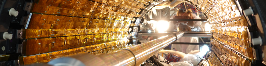
With its 10 m2 of active silicon area and nearly 13 billion pixels, the ITS2 is the largest pixel detector ever built. It is also the first detector at the LHC to use monolithic active pixel sensors (MAPS), instead of the more conventional and well-established hybrid pixels and silicon microstrips.
Change of scale
The particle sensors and the associated read-out electronics used for vertexing and tracking detection systems in particle-physics experiments have very demanding requirements in terms of granularity, material thickness, readout speed and radiation hardness. The development of sensors based on silicon-semiconductor technology and read-out integrated circuits based on CMOS technology revolutionised the implementation of such detection systems. The development of silicon microstrips, already successfully used at the Large Electron-Positron (LEP) collider, and, later, the development of hybrid pixel detectors, enabled the construction of tracking and vertexing detectors that meet the extreme requirements – in terms of particle rates and radiation hardness – set by the LHC. As a result, silicon microstrip and pixel sensors are at the heart of the particle-tracking systems in most particle-physics experiments today.
Nevertheless, compromises exist in the implementation of this technology. Perhaps the most significant is the interface between the sensor and the readout electronics, which are typically separate components. To go beyond these limitations and construct detection systems with higher granularity and less material thickness requires the development of new technology. The optimal way to achieve this is to integrate both sensor and readout electronics to create a single detection device. This is the approach taken with CMOS active pixel sensors (APSs). Over the past 20 years, extensive R&D has been carried out on CMOS APSs, making this a viable option for vertexing and tracking detection systems in particle and nuclear physics, although their performance in terms of radiation hardness is not yet at the level of hybrid pixel detectors.
ALPIDE, which is the result of an intensive R&D effort, is the building block of the ALICE ITS2
The first large-scale application of CMOS APS technology in a collider experiment was the STAR PXL detector at Brookhaven’s Relativistic Heavy-Ion Collider in 2014 (CERN Courier October 2015 p6). The ALICE ITS2 has benefitted from significant R&D since then, in particular concerning the development of a more advanced CMOS imaging sensor, named ALPIDE, with a minimum feature size of 180 nm. This has led to a significant improvement in the field of MAPS for single-particle detection, reaching unprecedented performance in terms of signal/noise ratio, spatial resolution, material budget and readout speed.
ALPIDE sensors
ALPIDE, which is the result of an intensive R&D effort carried out by ALICE over the past eight years, is the building block of the ALICE ITS2. The chip is 15 × 30 mm2 in area and contains more than half a million pixels organised in 1024 columns and 512 rows. Its very low power consumption (< 40 mW/cm2) and excellent spatial resolution (~5 μm) are perfect for the inner tracker of ALICE.

In ALPIDE the sensitive volume is a 25 μm-thick layer of high-resistivity p-type silicon (> 1 kΩ cm) grown epitaxially on top of a standard (low-resistivity) CMOS wafer (see “ALPIDE journeys” figure). The electric charge generated by particles traversing the sensitive volume is collected by an array of n–p diodes reverse-biased with a positive potential (~1 V) applied on the n-well electrode and a negative potential (down to a minimum of –6 V) applied to the substrate (backside). The possibility of varying the reverse-bias voltage in the range 1 to 7 V allows control over the size of the depleted volume (the fraction of the sensitive volume where the charge is collected by drift due to the presence of an electric field) and, correspondingly, the charge-collection time. Measurements carried out on sensors with characteristics identical to ALPIDE have shown an average charge-collection time consistently below 15 ns for a typical reverse-bias voltage of 4 V. Applying reverse substrate bias to the ALPIDE sensor also increases the tolerance to non-ionising energy loss to well beyond 1013 1 MeV neq/cm2, which is largely sufficient to meet ALICE’s requirements.
Another important feature of ALPIDE is the use of a p-well to shield the full CMOS circuitry from the epitaxial layer. Only the n-well collection electrode is not shielded. The deep p-well prevents all other n-wells – which contain circuitry – from collecting signal charge from the epitaxial layer, and therefore allows the use of full CMOS and consequently more complex readout circuitry in the pixel. ALICE is the first experiment where this has been used to implement a MAPS with a pixel front-end (amplifier and discriminator) and a sparsified readout within the pixel matrix similar to hybrid sensors. The low capacitance of the small collection electrode (about 2 × 2 μm2), combined with a circuit that performs sparsified readout within the matrix without a free-running clock, keeps the power consumption as low as 40 nW per pixel.
ITS2 structure
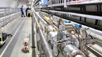
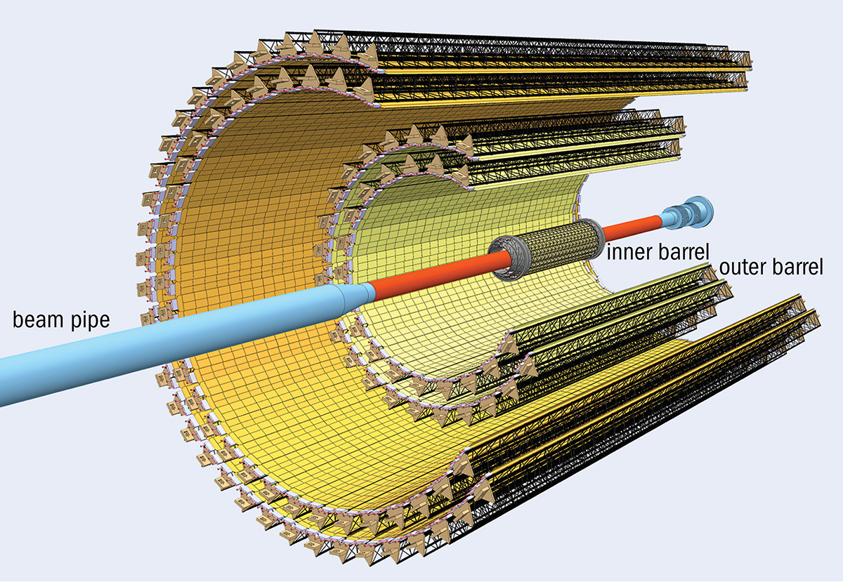
The ITS2 consists of seven layers covering a radial extension from 22 to 430 mm with respect to the beamline (see “Cylindrical structure” figure). The innermost three layers form the inner barrel (IB), while the middle two and the outermost two layers form the outer barrel (OB). The radial position of each layer was optimised to achieve the best combined performance in terms of pointing resolution, momentum resolution and tracking efficiency in the expected high track-density environment of a Pb–Pb collision. It covers a pseudo-rapidity range |η| < 1.22 for 90% of the most luminous beam interaction region, extending over a total surface of 10 m2 and containing about 12.5 Gpixels with binary readout, and is operated at room temperature using water cooling.
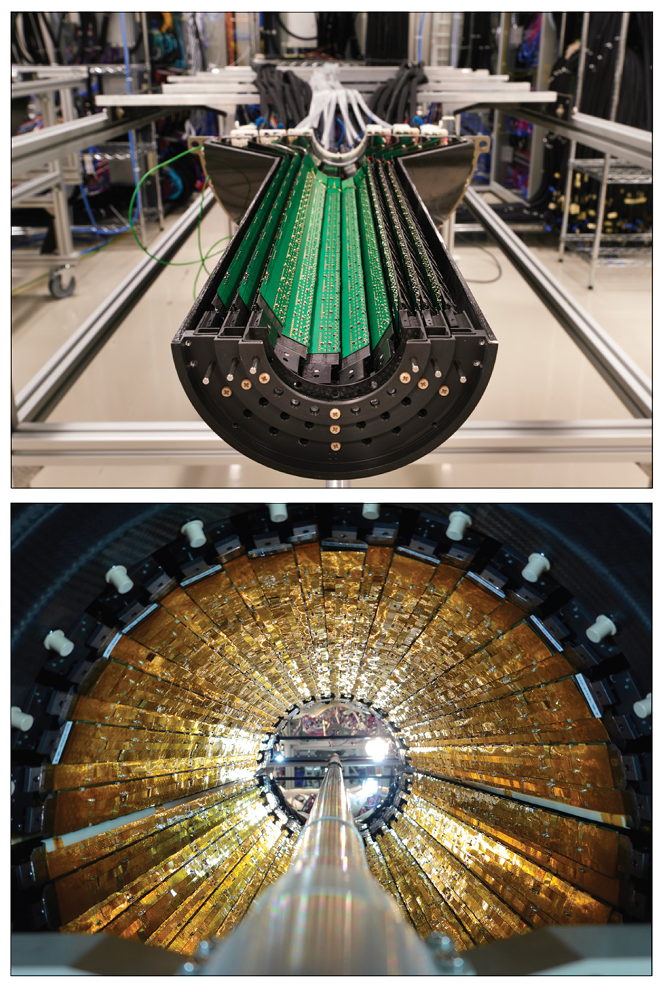
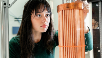
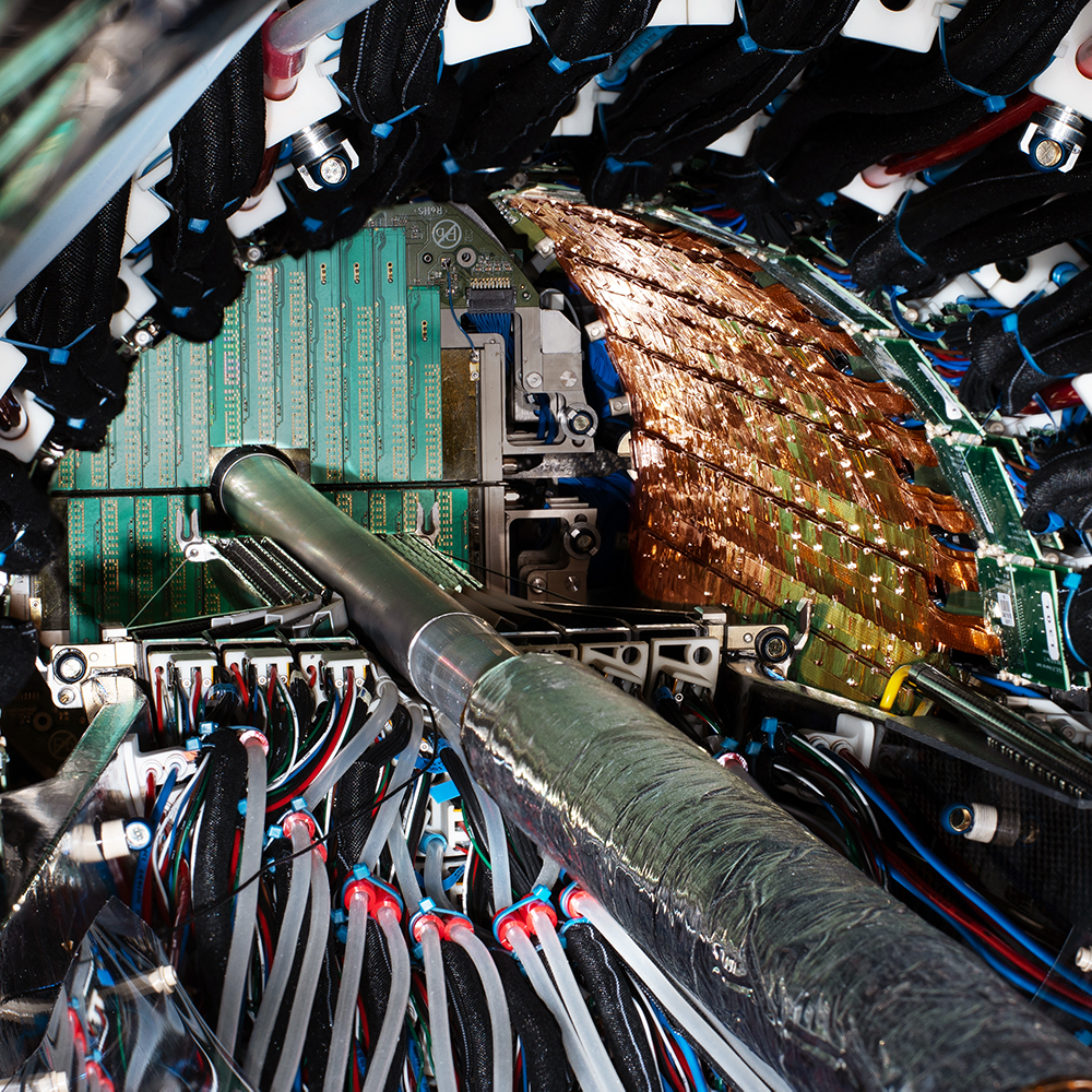
Given the small size of the ALPIDE (4.5 cm2), sensors are tiled-up to form the basic detector unit, which is called a stave. It consists of a “space-frame” (a carbon-fibre mechanical support), a “cold plate” (a carbon ply embedding two cooling pipes) and a hybrid integrated circuit (HIC) assembly in which the ALPIDE chips are glued and electrically connected to a flexible printed circuit. An IB HIC and an OB HIC include one row of nine chips and two rows of seven chips, respectively. The HICs are glued to the mechanical support: 1 HIC for the IB and 8 or 14 HICs for the two innermost and two outermost layers of the OB, respectively (see “State of the art” figure).
Zero-suppressed hit data are transmitted from the staves to a system of about 200 readout boards located 7 m away from the detector. Data is transmitted serially with a bit-rate up to 1.2 Gb/s over more than 3800 twin-axial cables reaching an aggregate bandwidth of about 2 Tb/s. The readout boards aggregate data and re-transmit it over 768 optical-fibre links to the first-level processors of the combined online/offline (O2) computing farm. The data are then sequenced in frames, each containing the hit information of the collisions occurring in contiguous time intervals of constant duration, typically 22 μs.
The process and procedures to build the HICs and staves are rather complex and time-intensive. More than 10 construction sites distributed worldwide worked together to develop the assembly procedure and to build the components. More than 120 IB and 2500 OB HICs were built using a custom-made automatic module-assembly machine, implementing electrical testing, dimension measurement, integrity inspection and alignment for assembly. A total of 96 IB staves, enough to build two copies of the three IB layers, and a total of 160 OB staves, including 20% spares, have been assembled.
A large cleanroom was built at CERN for the full detector assembly and commissioning activities. Here the same backend system that will be used in the experiment was installed, including the powering system, cooling system, full readout and trigger chains. Staves were installed on the mechanical support structures to form layers, and the layers are assembled in half-barrels, IB (layers 0, 1 and 2) top and bottom and OB (layers 3, 4, 5 and 6) top and bottom. Each stave is then connected to power-supply and readout systems. The commissioning campaign started in May 2019 to fully characterise and calibrate all the detector components, and installations of both the OB and IB were completed in May this year.
Physics ahead
After nearly 10 years of R&D, the upgrade of the ALICE experimental apparatus – which includes an upgraded time projection chamber, a new muon forward tracker, a new fast-interaction trigger detector, forward diffraction detector, new readout electronics and an integrated online–offline computing system – is close to completion. Most of the new or upgraded detectors, including the ITS2, have already been installed in the experimental area and the global commissioning of the whole apparatus will be completed this year, well before the start of Run 3, which is scheduled for the spring of 2022.
The significant enhancements to the performance of the ALICE detector will enable the exploration of new phenomena
The significant enhancements to the performance of the ALICE detector will enable detailed, quantitative characterisation of the high-density, high-temperature phase of strongly interacting matter, together with the exploration of new phenomena. The ITS2 is at the core of this programme. With improved pointing resolution and tracking efficiency at low transverse momentum, it will enable the determination of the total production cross-section of the charm quark. This is fundamental for understanding the interplay between the production of charm quarks in the initial hard scattering, their energy loss in the QGP and possible in-medium thermal production. Moreover, the ITS2 will also make it possible to measure a larger number of different charmed and beauty hadrons, including baryons, opening the possibility for determining the heavy-flavour transport coefficients. A third area where the new ITS will have a major impact is the measurement of electron–positron pairs emitted as thermal radiation during all stages of the heavy-ion collision, which offer an insight into the bulk properties and space–time evolution of the QGP.
More in store
The full potential of the ALPIDE chip underpinning the ITS2 is yet to be fully exploited. For example, a variant of ALPIDE explored by ALICE based on an additional low-dose deep n-type implant to realise a planar junction in the epitaxial layer below the wells containing the CMOS circuitry results in a much faster charge collection and significantly improved radiation hardness, paving the way for sensors that are much more resistant to radiation.

Further improvements to MAPS for high-energy physics detectors could come by exploiting the rapid progress in imaging for consumer applications. One of the features offered recently by CMOS imaging sensor technologies, called stitching, will enable a new generation of MAPS with an area up to the full wafer size. Moreover, the reduction in the sensor thickness to about 30–40 μm opens the door to large-area curved sensors, making it possible to build a cylindrical layer of silicon-only sensors with a further significant reduction in the material thickness. The ALICE collaboration is already preparing a new detector based on these concepts, which consists of three cylindrical layers based on curved wafer-scale stitched sensors (see “Into the future” figure). This new vertex detector will be installed during Long Shutdown 3 towards the middle of the decade, replacing the three innermost layers of the ITS2. With the first detection layer closer to the interaction point (from 23 to 18 mm) and a reduction in the material budget close to the interaction point by a factor of six, the new vertex detector will further improve the tracking precision and efficiency at low transverse momentum.
The technologies developed by ALICE for the ITS2 detector are now being used or considered for several other applications in high-energy physics, including the vertex detector of the sPHENIX experiment at RHIC, and the inner tracking system for the NICA MPD experiment at JINR. The technology is also being applied to areas outside of the field, including in medical and space applications. The Bergen pCT collaboration and INFN Padova’s iMPACT project, for example, are developing novel ALPIDE-based devices for clinical particle therapy to reconstruct 3D human body images. The HEPD02 detector for the Chinese–Italian CSES-02 mission, meanwhile, includes a charged-particle tracker made of three layers of ALPIDE sensors that represents a pioneering test for next-generation space missions. Driven by a desire to learn more about the fundamental laws of nature, it is clear that advanced silicon-tracker technology continues to make an impact on wider society, too.
Further reading
B Abelev et al. 2014 J. Phys. G 41 087002.
G Aglieri et al. 2013 JINST 8 C12041.
G Aglieri et al. 2021 Nucl. Instrum. Meth. A 988 164859.
W Snoeys et al. 2017 Nucl. Instrum. Meth. A 871 90.