An EU project is enabling detector solutions for upgraded and future accelerators.
Research in high-energy physics at particle accelerators requires highly complex detectors to observe the particles and study their behaviour. In the EU-supported project on Advanced European Infrastructure for Detectors at Accelerators (AIDA), more than 80 institutes from 23 European countries have joined forces to boost detector development for future particle accelerators in line with the European Strategy for Particle Physics. These include the planned upgrade of the LHC, as well as new linear colliders and facilities for neutrino and flavour physics. To fulfil its aims, AIDA is divided into three main activities: networking, joint research and transnational access, all of which are progressing well two years after the project’s launch.
Networking
AIDA’s networking activities fall into three work packages (WPs): the development of common software tools (WP2); microelectronics and detector/electronics integration (WP3); and relations with industry (WP4).
Building on and extending existing software and tools, the WP2 network is creating a generic geometry toolkit for particle physics together with tools for detector-independent reconstruction and alignment. The design of the toolkit is shaped by the experience gained with detector-description systems implemented for the LHC experiments – in particular LHCb – as well as by lessons learnt from various implementations of geometry-description tools that have been developed for the linear-collider community. In this context, the Software Development for Experiments and LHCb Computing groups at CERN have been working together to develop a new generation of software for geometry modellers. These are used to describe the geometry and material composition of the detectors and as the basis for tracking particles through the various detector layers.
Enabling the community to access the most advanced semiconductor technologies is an important aim for AIDA
This work uses the geometrical models in Geant4 and ROOT to describe the experimental set-ups in simulation or reconstruction programmes and involves the implementation of geometrical solid primitives as building blocks for the description of complex detector arrangements. These include a large collection of 3D primitives, ranging from simple shapes such as boxes, tubes or cones to more complex ones, as well as their Boolean combinations. Some 70–80% of the effort spent on code maintenance in the geometry modeller is devoted to improving the implementation of these primitives. To reduce the effort required for support and maintenance and to converge on a unique solution based on high-quality code, the AIDA initiative has started a project to create a “unified-solids library” of the geometrical primitives.
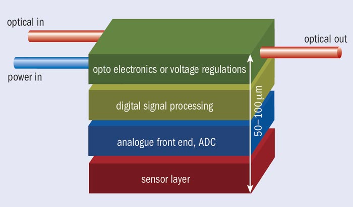
Enabling the community to access the most advanced semiconductor technologies – from nanoscale CMOS to innovative interconnection processes – is an important aim for AIDA. One new technique is 3D integration, which has been developed by the microelectronic industry to overcome limitations of high-frequency microprocessors and high-capacity memories. It involves fabricating devices based on two or more active layers that are bonded together, with vertical interconnections ensuring the communication between them and the external world. The WP3 networking activity is studying 3D integration to design novel tracking and vertexing detectors based on high-granularity pixel sensors.
Interesting results have already emerged from studies with the FE-Ix series of CMOS chips that the ATLAS collaboration has developed for the read-out of high-resistivity pixel sensors – 3D processing is currently in progress on FE-I4 chips. Now, some groups are evaluating the possibility of developing new electronic read-out chips in advanced CMOS technologies, such as 65 nm and of using these chips in a 3D process with high-density interconnections at the pixel level. Once the feasibility of such a device is demonstrated, physicists should be able to design a pixel detector with highly aggressive and intelligent architectures for sensing, analogue and digital processing, storage and data transmission (figure 1).
The development of detectors using breakthrough technologies calls for the involvement of hi-tech industry. The WP4 networking activity aims to increase industrial involvement in key detector-developments in AIDA and to provide follow-up long after completion of the project. To this end, it has developed the concept of workshops tailored to maximize the attendees’ benefits while also strengthening relations with European industry, including small and medium-sized enterprises (SMEs). The approach is to organize “matching events” that address technologies of high relevance for detector systems and gather key experts from industry and academia with a view to establish high-quality partnerships. WP4 is also developing a tool called “collaboration spotting”, which aims to monitor through publications and patents the industrial and academic organizations that are active in the technologies under focus at a workshop and to identify the key players. The tool was used successfully to invite European companies – including SMEs – to attend the workshop on advanced interconnections for chip packaging in future detectors that took place in April at the Laboratori Nazionali di Frascati of INFN.
Test beams and telescopes
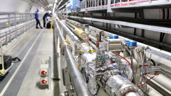
The development, design and construction of detectors for particle-physics experiments are closely linked with the availability of test beams where prototypes can be validated under realistic conditions or production modules can undergo calibration. Through its transnational access and joint research activities, AIDA is not only supporting test-beam facilities and corresponding infrastructures at CERN, DESY and Frascati but is also extending them with new infrastructures. Various sub-tasks cover the detector activities for the LHC and linear collider, as well as a neutrino activity, where a new low-energy beam is being designed at CERN, together with prototype detectors.
One of the highlights of WP8 is the excellent progress made towards two new major irradiation facilities at CERN
One of the highlights of WP8 is the excellent progress made towards two new major irradiation facilities at CERN. These are essential for the selection and qualification of materials, components and full detectors operating in the harsh radiation environments of future experiments. AIDA has strongly supported the initiatives to construct GIF++ – a powerful γ irradiation facility combined with a test beam in the North Area – and EAIRRAD, which will be a powerful proton and mixed-field irradiation facility in the East Area. AIDA is contributing to both projects with common user-infrastructure as well as design and construction support. The aim is to start commissioning and operation of both facilities following the LS1 shutdown of CERN’s accelerator complex.
The current shutdown of the test beams at CERN during LS1 has resulted in a huge increase in demand for test beams at the DESY laboratory. The DESY II synchrotron is used mainly as a pre-accelerator for the X-ray source PETRA III but it also delivers electron or positron beams produced at a fixed carbon-fibre target to as many as three test-beam areas. Its ease of use makes the DESY test beam an excellent facility for prototype testing because this typically requires frequent access to the beam area. In 2013 alone, 45 groups from more than 30 countries with about 200 users have already accessed the DESY test beams. Many of them received travel support from the AIDA Transnational Access Funds and so far AIDA funding has enabled a total of 130 people to participate in test-beam campaigns. The many groups using the beams include those from the ALICE, ATLAS, Belle II, CALICE, CLIC, CMS, Compass, LHCb, LCTPC and Mu3e collaborations.
About half of the groups using the test beam at DESY have taken advantage of a beam telescope to provide precise measurements of particle tracks. The EUDET project – AIDA’s predecessor in the previous EU framework programme (FP6) – provided the first beam telescope to serve a large user community, which was aimed at detector R&D for an international linear collider. For more than five years, this telescope, which was based on Minimum Ionizing Monolithic Active pixel Sensors (MIMOSA), served a large number of groups. Several copies were made – a good indication of success – and AIDA is now providing continued support for the community that uses these telescopes. It is also extending its support to the TimePix telescope developed by institutes involved in the LHCb experiment.
The core of AIDA’s involvement lies in the upgrade and extension of the telescope. For many users who work on LHC applications, a precise reference position is not enough. They also need to know the exact time of arrival of the particle but it is difficult to find a single system that can provide both position and time at the required precision. Devices with a fast response tend to be less precise in the spatial domain or put too much material in the path of the particle. So AIDA combines two technologies: the thin MIMOSA sensors with their spatial resolution provide the position; while the ATLAS FEI4 detectors provide time information with the desired LHC structure.
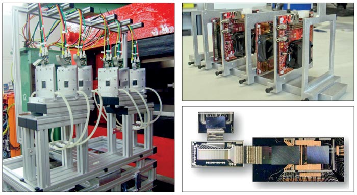
The first beam test in 2012 with a combined MIMOSA-FEI4 telescope was an important breakthrough. Figure 2 shows the components involved in the set-up in the DESY beam. Charged particles from the accelerator – electrons in this case – first traverse three read-out planes of the MIMOSA telescope, followed by the device under test, then the second triplet of MIMOSA planes and then the ATLAS-FEI4 arm. The DEPFET pixel-detector international collaboration was the first group to use the telescope, so bringing together within a metre pixel detectors from three major R&D collaborations.
While combining the precise time information from the ATLAS-FEI4 detector with the excellent spatial resolution of MIMOSA provides the best of both worlds, there is an additional advantage: the FEI4 chip has a self-triggering capability because it can issue a trigger signal based on the response of the pixels. Overlaying the response of the FEI4 pixel matrix with a programmable mask and feeding the resulting signal into the trigger logic allows triggering on a small area and is more flexible than a traditional trigger based on scintillators. To change the trigger definition, all that is needed is to upload a new mask to the device. This turns out to be a useful feature if the prototypes under test cover a small area.
Calorimeter development in AIDA WP9 is mainly motivated by experiments at possible future electron–positron colliders, as defined in the International Linear Collider and Compact Linear Collider studies. These will demand extremely high-performance calorimetry, which is best achieved using a finely segmented system that reconstructs events using the so-called particle-flow approach to allow the precise reconstruction of jet energies. The technique works best with an optimal combination of tracking and calorimeter information and has already been applied successfully in the CMS experiment. Reconstructing each particle individually requires fine cell granularity in 3D and has spurred the development of novel detection technologies, such as silicon photo-multipliers (SiPMs) mounted on small scintillator tiles or strips, gaseous detectors (micro mesh or resistive plate chambers) with 2D read-out segmentation and large-area arrays of silicon pads.
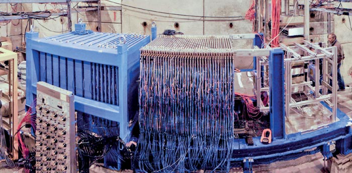
After tests of sensors developed by the CALICE collaboration in a tungsten stack at CERN (figure 3) – in particular to verify the neutron and timing response at high energy – the focus is now on the realization of fully technological prototypes. These include power-pulsed embedded data-acquisition chips requested for the particle-flow-optimized detectors for a future linear collider and they address all of the practical challenges of highly granular devices – compactness, integration, cooling and in situ calibration. Six layers (256 channels each) of a fine granularity (5 × 5 mm2) silicon-tungsten electromagnetic calorimeter are being tested in electron beams at DESY this July (figure 4). At the same time, the commissioning of full-featured scintillator hadron calorimeter units (140 channels each) is progressing at a steady pace. A precision tungsten structure and read-out chips are also being prepared for the forward calorimeters to test the radiation-hard sensors produced by the FCAL R&D collaboration.
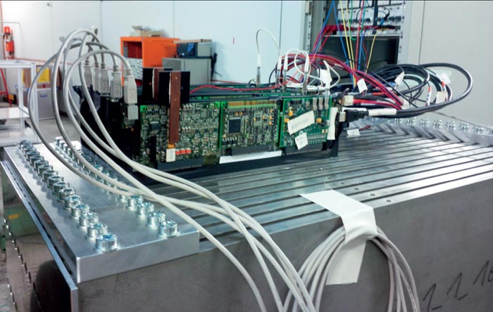
Image credit: DESY.
The philosophy behind AIDA is to bring together institutes to solve common problems so that once the problem is solved, the solution can be made available to the entire community. Two years on from the project’s start – and halfway through its four-year lifetime – the highlights described here, from software toolkits to a beam-telescope infrastructure to academia-industry matching, illustrate well the progress that is being made. Ensuring the user support of all equipment in the long term will be the main task in a new proposal to be submitted next year to the EC’s Horizon 2020 programme. New innovative activities to be included will be discussed during the autumn within the community at large.