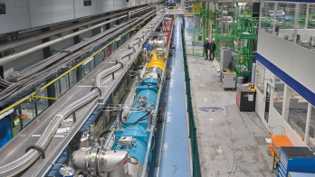
Plasma-driven thin-film deposition is routinely deployed for re-engineering the surface properties of vacuum beam pipes, chambers and components in particle accelerators. CERN’s Paolo Chiggiato, Pedro Costa Pinto and Guillaume Jonathan Rosaz explore the critical role that surface modification plays in large-scale vacuum systems.
Within a particle accelerator, the surface of materials directly exposed to the beams interacts with the circulating particles and, in so doing, influences the local vacuum conditions through which those particles travel. Put simply: accelerator performance is linked inextricably to the surface characteristics of the vacuum beam pipes and chambers that make up the machine.
In this way, the vacuum vessel’s material top surface and subsurface layer (just a few tens of nm thick) determine, among many other characteristics, the electrical resistance of the beam image current, synchrotron light reflectivity, degassing rates and secondary electron yield under particle bombardment. The challenge for equipment designers and engineers is that while the most common structural materials used to fabricate vacuum systems – stainless steel, aluminium alloys and copper – ensure mechanical resistance against atmospheric pressure, they do not deliver the full range of chemical and physical properties required to achieve the desired beam performance.
Sputtering is one of the methods used to produce thin films by physical vapour deposition
Aluminium alloys, though excellent in terms of electrical conductivity, suffer from high secondary electron emission. On the latter metric, copper represents a better choice, but can be inadequate regarding gas desorption and mechanical performance. Even though it is the workhorse of vacuum technology, for its excellent mechanical and metallurgical behaviour, stainless steel lacks most of the required surface properties. The answer is clear: adapt the surface properties of these structural materials to the specific needs of the accelerator environment by coating them with more suitable materials, typically using electrochemical or plasma treatments. (For a review of electrochemical coating methods, see Surface treatment: secrets of success in vacuum science.)
Variations on the plasma theme
The emphasis herein is exclusively on plasma-based thin-film deposition, in which an electrically quasi-neutral state of matter (composed of positive and negative charged particles) is put to work to re-engineer the physical and chemical properties of vacuum component/subsystem surfaces. A plasma can be produced by ionising gas atoms so that the positive charges are ions, and the negative ones are electrons. The most useful properties of the resultant gas plasma derive from the large difference in inertial mass between the particles carrying negative and positive charges. Owing to their much lower inertial mass, electrons are a lot more responsive than ions to variations of the electromagnetic field, leading to separation of charges and electrical fields within the plasma. What’s more, the particle trajectories for ions and electrons also differ markedly.
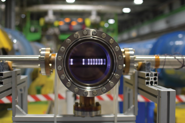
These characteristics can be exploited to deposit thin films and, more generally, to modify the properties of vacuum chamber and component surfaces. For such a purpose, noble-gas ions are extracted from a plasma and accelerated towards a negatively charged solid target. If the ions acquire enough kinetic energy (of the order of hundreds to thousands of eV), one of the effects of the bombardment is the extraction of neutral atoms from the target and their deposition on the surface of the substrate to be modified. This mechanism – called sputtering – is one of the methods used to produce thin films by physical vapour deposition (PVD), where film materials are extracted from a solid into a gas phase before condensing on a substrate.
In the plasma, the lost ions are reintroduced by electron ionisation of additional gas atoms. While the rate of ionisation is improved by increasing the gas density, an excessive gas density can have a detrimental effect on the sputtered atoms (as their trajectories are modified and their kinetic energy decreased by multiple collisions with gas atoms). The alternative is to increase the length of the electron trajectories by applying a magnetic field of several hundred gauss to the plasma.
Contrary to ions – which are affected minimally – electrons move around the lines of force of the magnetic field in longer helical-like curves, such that the probability of hitting an atom is higher. As electrons are sooner or later lost – either on the growing film or nearby surfaces – the plasma is refilled by secondary electrons extracted from the target (as a result of ion collisions). For a given set of parameters – among them target voltage, plasma power, gas pressure and magnetic flux density – the plasma ultimately attains stable conditions and a constant rate of deposition. Typical film thicknesses for accelerator applications range from a few tens of nm to 2–3 microns.
Unique requirements
The peculiarities of thin-film deposition for accelerator applications lie in the size of the objects to be coated and the purity of the coatings in question. Substrate areas, for example, range from a few cm2 up to m2, and in a great variety of 3D shapes and geometries. Large-aspect-ratio beam pipes that are several metres long or complicated multicell cavities for RF applications are typical substrates regularly coated at CERN. The coating process is implemented either in dedicated workshops or directly inside the accelerators during the retrofitting of installed equipment.
HiPIMS target geometries and coating parameters must be optimised for each family of accelerator components
The simplest sputtering configuration can be deployed when coating a cylindrical beam pipe. The target, which is made of a wire or a rod of the material to be deposited, is aligned along the longitudinal axis of the beam pipe. Argon is the most commonly used noble gas, at a pressure that depends on the cross-section – i.e. the smaller the diameter, the higher the pressure (a typical value for vacuum chambers that are a few centimetres in diameter is 0.1 mbar). The plasma is ignited by polarising the target negatively (at a few hundred volts) using a DC power supply while keeping the pipe grounded. It’s possible to reduce the pressure by one or two orders of magnitude if a magnetic field is applied parallel to the target (owing to the longer electron paths). In this case, the deposition technique is known as DC magnetron sputtering.
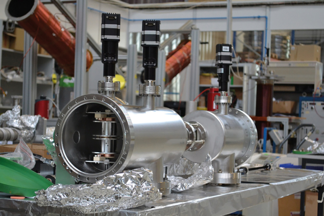
When the substrate is not a simple cylinder, however, the target design becomes more complicated. That’s because of the need to accommodate different target–substrate distances, while the angle of incidence of sputtered atoms on the substrate is also subject to change. As a result, the deposited film might have different thicknesses and uneven properties at different locations on the substrate (owing to dissimilar morphologies, densities and defects, including voids). These weaknesses have been addressed, in large part, over recent years with a new family of sputtering methods called high-power impulse magnetron sputtering (HiPIMS).
In HiPIMS, short plasma pulses (of the order of 10-100 μs) of high power density (kW/cm2 regime) are applied to the target. The discharge is shut down between two consecutive pulses for a duration of about 100–1000 μs; in this way, the duty cycle is low (less than 10%) and the average power ensures there is no overheating and deformation of the target. The resulting plasma, though, is about 10 times denser (approximately 1013 ions/cm3) versus standard DC magnetron sputtering – a figure of merit that, thanks to a bias voltage applied to the substrate, ensures a higher fraction of ionised sputtered atoms are transported to the surfaces to be coated.
The impingement of such energetic ions produces denser films and reduces the columnar structure resulting from the deposition of sputtered atoms moving along lines of sight. As the bias voltage is not always a safe and practical solution, the CERN vacuum team has successfully tested the application of a positive pulse to the target immediately after the main negative pulse. The effect is an increase in energy of the ionised sputtered atoms, with equivalent results as per the bias voltage (though with a simpler implementation for accelerator components).
Owing to the variety of materials and shapes encountered along a typical (or atypical) beamline, the HiPIMS target geometries and coating parameters must be optimised for each distinct family of accelerator components. This optimisation phase is traditionally experimental, based on testing and measurement of “coupon samples” and then prototypes. In the last five years, however, the CERN team has reinforced these experimental studies with 3D simulations based on a particle-in-cell Monte Carlo/direct simulation Monte Carlo (PICMS/DSMC) code – a capability originally developed at the Fraunhofer Institute for Surface Engineering and Thin Films (IST) in Braunschweig, Germany.
Surface cleaning: putting plasmas to work
Notwithstanding their central role in thin-film deposition, plasmas are also used at CERN to clean surfaces for vacuum applications and to enhance the adherence of thin films. A case in point is the application of plasmas containing oxygen ions and free radicals (highly reactive chemical species) for the removal of hydrocarbons. In short: the ions and radicals are driven toward the contaminated surface, where they can decompose hydrocarbon molecules and form volatile species (e.g. CO and CO2) for subsequent evacuation.
It’s a method regularly used to clean beryllium surfaces (which cannot be treated by traditional chemical methods for safety reasons). If the impingement kinetic energy of the oxygen ions is about 100 eV, the chemical reaction rate on the surface is much larger than the beryllium sputtering rate, such that cleaning is possible without producing hazardous compounds of the carcinogenic metal.
Meanwhile, plasma treatments have recently been proposed for the cleaning of stainless-steel radioactive components when they are dismounted from accelerators, modified and then reinstalled. Using a remote plasma source, the energy of the plasma’s oxygen ions is chosen (<50 eV) so as to avoid sputtering of the component materials, thereby preventing radioactive atoms from entering the gas phase. The main difficulty here is to adapt the plasma source to the wealth of different geometries that are typical of accelerator components.
Plasma versatility
So much for the fundamentals of plasma processing, what of the applications? At CERN, the large-scale deployment of thin-film coatings began in the 1980s on the Large Electron–Positron (LEP) collider. To increase LEP’s collision energy to 200 GeV and above, engineering teams studied, and subsequently implemented, superconducting niobium (Nb) thin films deposited on copper (Cu) for the RF cavities (in place of bulk niobium).
This technology was also adopted for the Large Hadron Collider (LHC), the High Intensity and Energy ISOLDE (HIE ISOLDE) project at CERN and other European accelerators operating at fields up to 15 MV/m. The advantages are clear: lower cost, better thermal stability (thanks to the higher thermal conductivity of the copper substrate), and reduced sensitivity to trapped magnetic fields. The main drawback of Nb/Cu superconducting RF cavities is an exponential growth of the power lost in an RF cycle with the accelerating electrical field (owing to resistivity and magnetic permeability of the Nb film). This weakness, although investigated extensively, has eluded explanation and proposed mitigation for the past 20 years.
NEG coatings comprise a mixture of titanium, zirconium and vanadium
It’s only lately, in the frame of studies for the proposed electron–positron Future Circular Collider (FCC-ee), that researchers have shed light on this puzzling behaviour. Those insights are due, in large part, to a deeper theoretical analysis of Nb thin-film densification as a result of HiPIMS, though a parallel line of investigation involves the manufacturing of seamless copper cavities and their surface electropolishing. In both cases, the objective is the reduction of defects in the substrate to enhance film adherence and purity.
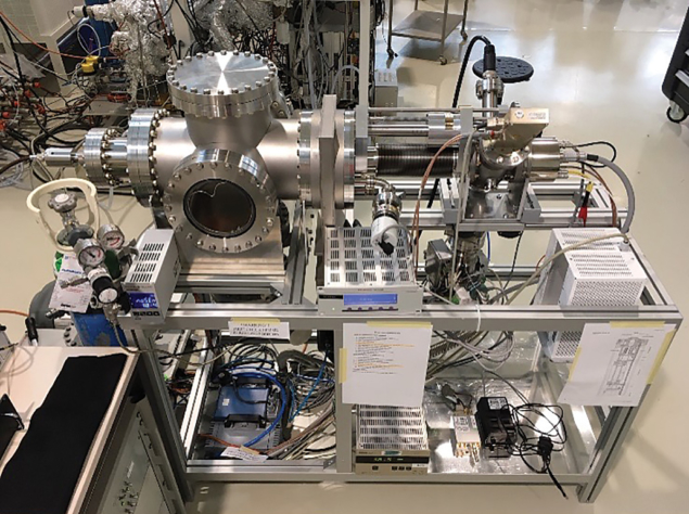
Related studies have shown that Nb films on Cu can perform as well as bulk Nb in terms of superconducting RF properties, though coating materials other than Nb are also under investigation. Today, for example, the CERN vacuum group is evaluating Nb3Sn and V3Si – both of which are part of the A15 crystallographic group and exhibit superconducting transition temperatures of about 18 K (i.e. 9 K higher than Nb). This higher critical temperature would allow the use of RF cavities operating at 4.3 K (instead of 1.9 K), yielding significant simplification of the cryogenic infrastructure and reductions in electrical energy consumption. Even so, intense development is still necessary before these coatings can really challenge pure Nb films – not least because A15 films are brittle, plus the coating of such materials is tricky (given the need to reproduce a precise stoichiometry and crystallographic structure).
Game-changing innovations
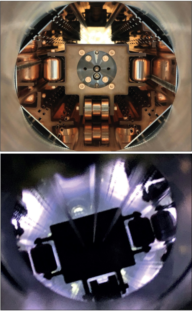
Another wide-scale application of plasma processing at CERN is in the deposition of non-evaporable-getter (NEG) thin-film coatings, specialist materials originally developed to provide distributed vacuum pumping for the LHC. NEG coatings comprise a mixture of titanium, zirconium and vanadium with a typical composition around 30:30:40, respectively. For plasma deposition of NEG films, the target (comprising three interlacing elemental wires) is pulled along the main axis of the beam pipes. Once the coated vacuum chambers are installed within an accelerator and pumped out, the NEG films undergo heating for 24 hours at temperatures ranging from 180 to 250 °C – a process known as activation, in which the superficial oxide layer and any contaminants are dissolved into their bulk.
The clean surfaces obtained in this way chemically adsorb most of the gas species in the vacuum system at room temperature – except for noble gases (which are chemically inert) and methane (for which small auxiliary pumps are necessary). The NEG-coated surfaces provide an impressively high pumping speed and, thanks to their cleanliness, a lower desorption yield when bombarded by electrons, photons and ions – and all this with minimal space occupancy. Moreover, owing to their maximum secondary electron yields (δmax) below 1.3, NEG coatings avoid the development of electron multipacting, the main cause of electron clouds in beam pipes (and related unfavourable impacts on beam performance, equipment operation and cryogenic heat load).
More broadly, plasma processing of NEG coatings represents a transformative innovation in the implementation of large-scale vacuum systems. Hundreds of beam pipes were NEG-coated for the long straight section of the LHC, including the experimental vacuum chambers inserted in the four gigantic detectors. Beyond CERN, NEG coatings have also been employed widely in other large scientific instruments, including the latest generation of synchrotron light sources.
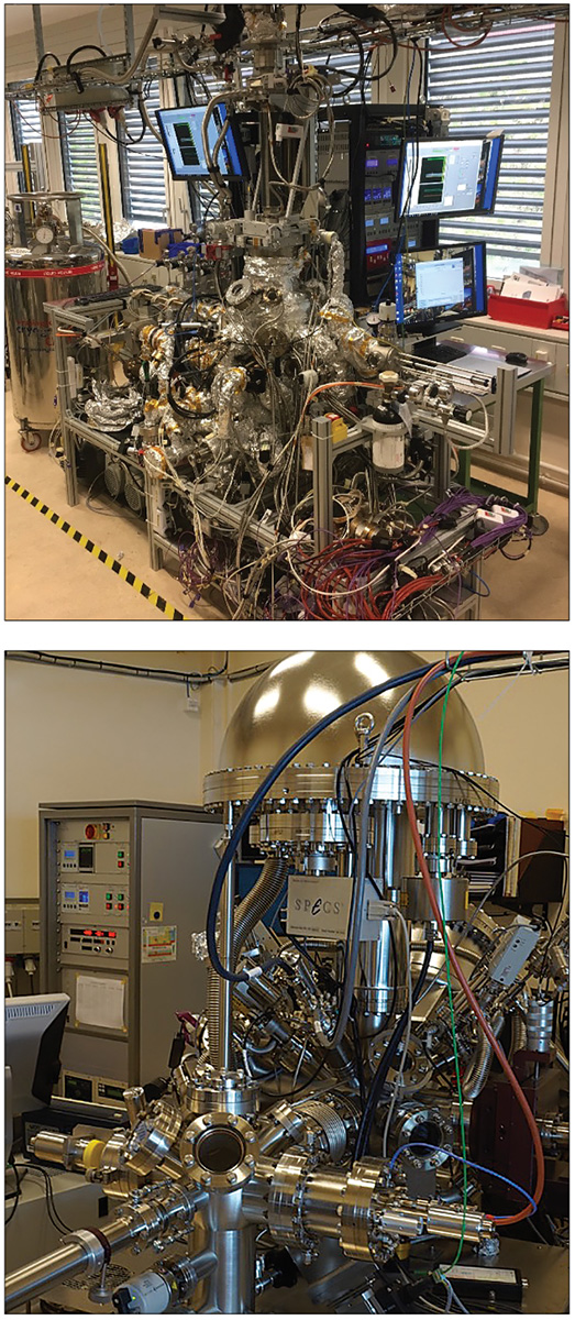
In-situ capabilities
Of course, NEG coatings require thermal activation, so cannot be applied in vacuum systems that are unheatable (i.e. vacuum vessels that operate at cryogenic temperatures or legacy accelerators that may need retrofitting). For these specific cases, the CERN vacuum team has, over the past 15 years, been developing and iterating low-δmax carbon coatings comprised mostly of amorphous carbon (a-C) with prevailing graphitic-like bonding among the carbon atoms.
Even though a-C thin films were originally studied for CERN’s older Super Proton Synchrotron (SPS), they are now the baseline solution for the beam screen of the superconducting magnets in the long straight section of the High-Luminosity LHC. A 100 nm thin coating is deposited either in the laboratory for the new magnets (located on both sides of the ATLAS and CMS detectors) or in situ for the ones already installed in the tunnel (both sides of LHCb and ALICE).
Production of denser plasmas will be key for future applications in surface treatments for accelerators
The in situ processing has opened up another productive line of enquiry: the possibility of treating the surface of beam screens (15 m long, a few cm diameter) directly in the accelerators with the help of mobile targets. The expectation is that these innovative coating methods for a-C could, over time, also be applied to improve the performance of installed vacuum chambers in the LHC’s arcs, without the need to dismount magnets and cryogenic connections.
Opportunity knocks
Looking ahead, the CERN vacuum team has plenty of ideas regarding further diversification of plasma surface treatments – though the direction of travel will ultimately depend on the needs of future studies, projects and collaborations. Near term, for example, there are possible synergies with the Advanced Proton Driven Plasma Wakefield Acceleration Experiment (AWAKE), an accelerator R&D project based at CERN that’s investigating the use of plasma wakefields driven by a proton bunch to accelerate charged particles over short distances. Certainly, the production of denser plasmas (and their manipulation) will be key for future applications in surface treatments for accelerators.
Another area of interest is the use of plasma-assisted chemical vapour deposition to extend the family of materials that can be deposited. For the longer term, the coating of vacuum systems with inert materials that allow the attainment of very low pressures (in the ultrahigh vacuum regime) in a short timeframe (five years) without bakeout remains one of the most ambitious targets.


