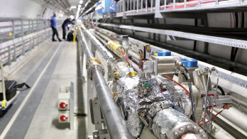
In the search for optimal performance under difficult conditions, experiments for CERN’s LHC are exploiting new technologies. One example is the large-scale use of avalanche photodiodes to read out light signals, which are produced by electromagnetically interacting particles in the CMS detector.
Photodiodes light-sensitive semiconductors have long been used in high-energy physics to read out signals from scintillating fibres and light-emitting crystals in calorimeters, because large magnetic fields or space may prevent the use of vacuum devices. One example is a simple pin photodiode with a layer of intrinsic semiconductor sandwiched between the p and n layers.
An advance on this basic configuration is the avalanche photodiode (APD). The applied bias voltage produces a region with a large field (150 kV/cm or more) in which to generate an avalanche of secondary carriers and thereby amplify the signal. This gain depends on both the applied field and the temperature. This technique has the additional advantage of fully amplifying the signal generated by the scintillation light absorbed at the surface, while signals generated within the diode by traversing ionizing particles are not amplified. A further refinement of the avalanche device is a “reverse” structure, first developed at the beginning of the 1990s, in which a thick avalanche region is located behind a thinner photoconversion layer (in contrast with a standard avalanche device in which the photoconversion layer is thicker).
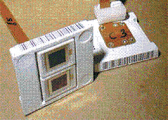
The scintillating crystals, which are used for recording electromagnetic energy, are one of the big spin-off success stories of particle physics. For big detectors, such as CMS at CERN’s LHC, lead tungstate facilitates a compact calorimeter design and produces short, fast signals. However, because lead tungstate has a low light yield, the APD read-out’s combination of amplification of the light signal and insensitivity to ionizing particles is crucial.
Developing APDs that were able to withstand the high particle intensities of the CMS environment required further research and development with two different specialist suppliers. Using more than 30 different APD prototypes, substantial progress was made and beam tests, using lead tungstate crystals, achieved the design energy resolution of better than 0.5%. The next task was to decide on the relative merits of manufacture, either via epitaxial growth or by diffusion. Last year, CMS chose the epitaxy route, and, after further development work, a contract with Hamamatsu for the supply of 130 000 APDs was signed in Japan by PSI (with ETHZ, Northeastern University and the universities of Minnesota and Split as contributing partners).
Meanwhile a full-scale CMS electromagnetic calorimeter module, with a 400 lead tungstate crystal read-out via 800 APDs, is being constructed at CERN.


