On-chip acceleration pioneers Robert Byer, Joel England, Peter Hommelhoff and Roy Shiloh report on progress to miniaturise accelerators from centimetres to microns.

Metal cavities are at the heart of the vast majority of the world’s 30,000 or so particle accelerators. Excited by microwaves, these resonant structures are finely tuned to generate oscillating electric fields that accelerate particles over many metres. But what if similar energies could be delivered 100 times more rapidly in structures a few tens of microns wide or less?
The key is to reduce the wavelength of the radiation powering the structure down to the optical scale of lasers. By combining solid-state lasers and modern nanofabrication, accelerating structures can be as small as a single micron wide. Though miniaturisation will never allow bunch charges as large as in today’s science accelerators, field strengths can be much higher before structure damage sets in. The trick is to replace highly conductive structures with dielectrics like silicon, fused silica and diamond, which have a much higher damage threshold at optical wavelengths. The length of accelerators can thereby be reduced by orders of magnitude, with millions to billions of particle pulses accelerated per second, depending on the repetition rate of the laser.
Recent progress with “on chip” accelerators promises powerful, high-energy and high-repetition-rate particle sources that are accessible to academic laboratories. Applications may range from localised particle or X-ray irradiation in medical facilities to quantum communication and computation using ultrasmall bunches of electrons as qubits.
Laser focused
The inspiration for on-chip accelerators dates back to 1962, when Koichi Shimoda of the University of Tokyo proposed using early lasers – then called optical masers – as a way to accelerate charged particles. The first experiments were conducted by shining light onto an open metal grating, generating an optical surface mode that could accelerate electrons passing above the surface. This technique was proposed by Yasutugu Takeda and Isao Matsui in 1968 and experimentally demonstrated by Koichi Mizuno in 1987 using terahertz radiation. In the 1980s, accelerator physicist Robert Palmer of Brookhaven National Laboratory proposed using rows of free-standing pillars of subwavelength separation illuminated by a laser – an idea that has propagated to modern devices.

In the 1990s, the groups of John Rosenzweig and Claudio Pellegrini at UCLA and Robert Byer at Stanford began to use dielectric materials, which offer low power absorption at optical frequencies. For femtosecond laser pulses, a simple dielectric such as silica glass can withstand optical field strengths exceeding 10 GV/m. It became clear that combining lasers with on-chip fabrication using dielectric materials could subject particles to accelerating forces 10 to 100 times higher than in conventional accelerators.
In the intervening decades, the dream of realising a laser-driven micro-accelerator has been enabled by major technological advances in the silicon-microchip industry and solid-state lasers. These industrial technologies have paved the way to fabricate and test particle accelerators made from silicon and other dielectric materials driven by ultrashort pulses of laser light. The dielectric laser accelerator (DLA) has been born.
Accelerator on a chip
Colloquially called an accelerator on a chip, a DLA is a miniature microwave accelerator reinvented at the micron scale using the methods of optical photonics rather
than microwave engineering. In both cases, the wavelength of the driving field determines the typical transverse structure dimensions: centimetres for today’s microwave accelerators, but between one and 10 μm for optically powered devices.
Other laser-based approaches to miniaturisation are available. In plasma-wakefield accelerators, particles gain energy from electromagnetic fields excited in an ionised gas by a high-power drive laser (CERN Courier May/June 2024 p25). But the details are starkly different. DLAs are powered by lasers with thousands to millions of times lower peak energy. They operate with more than a million times lower electron charges, but at millions of pulses per second. And unlike plasma accelerators, but similarly to their microwave counterparts, DLAs use a solid material structure with a vacuum channel in which an electromagnetic mode continuously imparts energy to the accelerated particles.

This mode can be created by a single laser pulse perpendicular to the electron trajectory, two pulses from opposite sides, or a single pulse directed downwards into the plane of the chip. The latter two options offer better field symmetry.
As the laser impinges on the structure, its electrons experience an electromagnetic force that oscillates at the laser frequency. Particles that are correctly matched in phase and velocity experience a forward accelerating force (see “Continuous acceleration” image). Just as the imparted force begins to change sign, the particles enter the next accelerating cycle, leading to continuous energy gain.
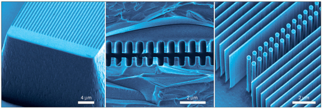
In 2013, two early experiments attracted international attention by demonstrating the acceleration of electrons using structured dielectric devices. Peter Hommelhoff’s group in Germany accelerated 28 keV electrons inside a modified electron microscope using a single-sided glass grating (see “Evolution” image, left panel). In parallel, at SLAC, the groups of Robert Byer and Joel England accelerated relativistic 60 MeV electrons using a dual-sided grating structure, achieving an acceleration gradient of 310 MeV/m and 120 keV of energy gain (see “Evolution” image, middle panel).
Teaming up
Encouraged by the experimental demonstration of accelerating gradients of hundreds of MeV/m, and the power efficiency and compactness of modern solid-state fibre lasers, in 2015 the Gordon and Betty Moore Foundation funded an international collaboration of six universities, three government laboratories and two industry partners to form the Accelerator on a Chip International Program (ACHIP). The central goal is to demonstrate a compact tabletop accelerator based on DLA technology. ACHIP has since developed “shoebox” accelerators on both sides of the Atlantic and used them to demonstrate nanophotonics-based particle control, staging, bunching, focusing and full on-chip electron acceleration by laser-driven microchip devices.
Silicon’s compatibility with established nanofabrication processes makes it convenient, but reaching gradients of GeV/m requires materials with higher damage thresholds such as fused silica or diamond. In 2018, ACHIP research at UCLA accelerated electrons from a conventional microwave linac in a dual-sided fused silica structure powered by ultrashort (45 fs) pulses of 800 nm wavelength laser light. The result was an average energy gain of 850 MeV/m and accelerating fields up to 1.8 GV/m – more than double the prior world best in a DLA, and still a world record.

Since DLA structures are non-resonant, the interaction time and energy gain of the particles is limited by the duration of the laser pulse. However, by tilting the laser’s pulse front, the interaction time can be arbitrarily increased. In a separate experiment at UCLA, using a laser pulse tilted by 45˚, the interaction distance was increased to more than 700 µm – or 877 structure periods – with an energy gain of 0.315 MeV. The UCLA group has further extended this approach using a spatial light modulator to “imprint” the phase information onto the laser pulse, achieving more than 3 mm of interaction at 800 nm, or 3761 structure periods.
Under ACHIP, the structure design has evolved in several directions, from single-sided and double-sided gratings etched onto substrates to more recent designs with colonnades of free-standing silicon pillars forming the sides of the accelerating channel, as originally proposed by Robert Palmer some 30 years earlier. At present, these dual-pillar structures (see “Evolution” image, right panel) have proven to be the optimal trade-off between cleanroom fabrication complexity and experimental technicalities. However, due to the lower damage threshold of silicon as compared with fused silica, researchers have yet to demonstrate gradients above 350 MeV/m in silicon-based devices.
With the dual-pillar colonnade chosen as the fundamental nanophotonic building block, research has turned to making DLAs into viable accelerators with much longer acceleration lengths. To achieve this, we need to be able to control the beam and manipulate it in space and time, or electrons quickly diverge inside the narrow acceleration channel and are lost on impact with the accelerating structure. The ACHIP collaboration has made substantial progress here in recent years.
Focusing on nanophotonics
In conventional accelerators, quadrupole magnets focus electron beams in a near perfect analogy to how concave and convex lens arrays transport beams of light in optics. In laser-driven nanostructures it is necessary to harness the intrinsic focusing forces that are already present in the accelerating field itself.
On-chip accelerators promise powerful, high-energy and high-repetition-rate particle sources that are accessible to academic laboratories
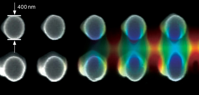
In 2021, the Hommelhoff group guided an electron pulse through a 200 nm-wide and 80 µm-long structure based on a theoretical lattice designed by ACHIP colleagues at TU Darmstadt three years earlier. The lattice’s alternating-phase focusing (APF) periodically exchanges an electron bunch’s phase-space volume between the transverse dimension across the narrow width of the accelerating channel and the longitudinal dimension along the propagation direction of the electron pulse. In principle this technique could allow electrons to be guided through arbitrarily long structures.
Guiding is achieved by adding gaps between repeating sets of dual-pillar building-blocks (see “Beam control” image). Combined guiding and acceleration has been demonstrated within the past year. To achieve this, we select a design gradient and optimise the position of each pillar pair relative to the expected electron energy at that position in the structure. Initial electron energies are up to 30 keV in the Hommelhoff group, supplied by electron microscopes, and from 60 to 90 keV in the Byer group, using laser-assisted field emission from silicon nanotips. When accelerated, the electrons’ velocities change dramatically from 0.3 to 0.7 times the speed of light or higher, requiring the periodicity of the structure to change by tens of nanometres to match the velocity of the accelerating wave to the speed of the particles.

Although focusing in the narrow dimension of the channel is the most critical requirement, an extension of this method to focus beams in the transverse vertical dimension out of plane of the chip has been proposed, which varies the geometry of the pillars along the out-of-plane dimension. Without it, the natural divergence of the beam in the vertical direction eventually becomes dominant. This approach is awaiting experimental realisation.
Acceleration gradients can be improved by optimising material choice, pillar dimensions, peak optical field strength and the duration of the laser pulses. In recent demonstrations, both the Byer and Hommelhoff groups have kept pillar dimensions constant to ease difficulties in uniformly etching the structures during nanofabrication. The complete structure is then a series of APF cells with tapered cell lengths and tapered dual-pillar periodicity. The combination of tapers accommodates both the changing size of the electron beam and the phase matching required due to the increasing electron energy.
In these proof-of-principle experiments, the Hommelhoff group has designed a nanophotonic dielectric laser accelerator for an injection energy of 28.4 keV and an average acceleration gradient of at least 22.7 MeV/m, demonstrating a 43% energy increase over a 500 µm-long structure. The Byer group recently demonstrated the acceleration of a 96 keV beam at average gradients of 35 to 50 MeV/m, reaching a 25% energy increase over 708 µm. The APF periods were in the range of tens of microns and were tapered along with the energy-gain design curve. The beams were not bunched, and by design only 4% of the electrons were captured and accelerated.
One final experimental point has important implications for the future use of DLAs as compact tabletop tools for ultrafast science. Upon interaction with the DLA, electron pulses have been observed to form trains of evenly spaced sub-wavelength attosecond-scale bunches. This effect was shown experimentally by both groups in 2019, with electron bunches measured down to 270 attoseconds, or roughly 4% of the optical cycle.
From demonstration to application
To date, researchers have demonstrated high gradient (GeV/m) acceleration, compatible nanotip electron sources, laser-driven focusing, interaction lengths up to several millimetres, the staging of multiple structures, and attosecond-level control and manipulation of electrons in nanophotonic accelerators. The most recent experiments combine these techniques, allowing the capture of an accelerated electron bunch with net acceleration and precise control of electron dynamics for the first time.
These milestone experiments demonstrate the viability of the nanophotonic dielectric electron accelerator as a scalable technology that can be extended to arbitrarily long structures and ever higher energy gains. But for most applications, beam currents need to increase.
A compelling idea proposes to “copy and paste” the accelerator design in the cleanroom and make a series of parallel accelerating channels on one chip. Another option is to increase the repetition rate of the driving laser by orders of magnitude to produce more electron pulses per second. Optimising the electron sources used by DLAs would also allow for more electrons per pulse, and parallel arrays of emitters on multi-channel devices promise tremendous advantages. Eventually, active nanophotonics can be employed to integrate the laser and electron sources on a single chip.
Once laser and electron sources are combined, we expect on-chip accelerators to become ubiquitous devices with wide-ranging and unexpected applications, much like the laser itself. Future applications will range from medical treatment tools to electron probes for ultrafast science. According to the International Atomic Energy Agency
statistics, 13% of major accelerator facilities around the world power light sources. On-chip accelerators may follow a similar path.
Illuminating concepts
A concept has been proposed for a dielectric laser-driven undulator (DLU) which uses laser light to generate deflecting forces that wiggle the electrons so that they emit coherent light. Combining a DLA and a DLU could take advantage of the unique time structure of DLA electrons to produce ultrafast pulses of coherent radiation (see “Compact light source” image). Such compact new light sources – small enough to be accessible to individual universities – could generate extremely short flashes of light in ultraviolet or even X-ray wavelength ranges, enabling tabletop instruments for the study of material dynamics on ultrafast time scales. Pulse trains of attosecond electron bunches generated by a DLA could provide excellent probes of transient molecular electronic structure.
The generation of intriguing quantum states of light might also be possible with nanophotonic devices
The generation of intriguing quantum states of light might also be possible with nanophotonic devices. This quantum light results from shaping electron wavepackets inside the accelerator and making them radiate, perhaps even leading to on-chip quantum-communication light sources.
In the realm of medicine, an ultracompact self-contained multi-MeV electron source based on integrated photonic particle accelerators could enable minimally invasive cancer treatments with improved dose control.
One day, instruments relying on high-energy electrons produced by DLA technology may bring the science of large facilities into academic-scale laboratories, making novel science endeavours accessible to researchers across various disciplines and minimally invasive medical treatments available to those in need. These visionary applications may take decades to be fully realised, but we should expect developments to continue to be rapid. The biggest challenges will be increasing beam power and transporting beams across greater energy gains. These need to be addressed to reach the stringent beam quality and machine requirements of longer term and higher energy applications.
Further reading
R Shiloh et al. 2021 Nature 597 498.
R Shiloh et al. 2022 Adv. Opt. Phot. 14 862.
T Chlouba et al. 2023 Nature 622 476.
P Broaddus et al. 2024 Phys. Rev. Lett. 132 085001.


