Ever since its discovery in 1995 at the Tevatron, the top quark has been considered to be a highly effective probe of new physics. A key reason is that the last fundamental fermion predicted by the Standard Model (SM) has a remarkably high mass, just a sliver under the Higgs vacuum expectation value divided by the square root of two, implying a Yukawa coupling close to unity. This has far-reaching implications: the top quark impacts the electroweak sector significantly through loop corrections, and may couple preferentially to new massive states. But while the top quark may represent a window into new physics, we cannot know a priori whether new massive particles could ever be produced at the LHC, and direct searches have so far been inconclusive. Model-independent measurements carried out within the framework of effective field theory (EFT) are therefore becoming increasingly important as a means to make the most of the wealth of precision measurements at the LHC. This approach makes it possible to systematically correlate sparse deviations observed in different measurements, in order to pinpoint any anomalies in top-quark couplings that might arise from unknown massive particles.
The top quark impacts the electroweak sector significantly through loop corrections
A new CMS analysis searches for anomalies in top-quark interactions with the Z boson using an EFT framework. The cross-section measurements of the rare associated production of either one (tZ) or two (ttZ) top quarks with a Z boson were statistically limited until recently. These interactions are among the least constrained by the available data in the top-quark sector, despite being modified in numerous beyond-SM models, such as composite Higgs models and minimal supersymmetry. Using the full LHC Run-2 data set, this study targets high-purity final states with multiple electrons and muons. It sets some of the tightest constraints to date on five generic types of EFT interactions that could substantially modify the characteristics of associated top-Z production, while having negligible or no effect on background processes.
Machine learning
In contrast to the more usual reinterpretations of SM measurements that require assumptions on the nature of new physics, this analysis considers EFT effects on observables at the detector level and constrains them directly from the data using a strategy that combines observables specifically selected for their sensitivity to EFT. The key feature of this work is its heavy use of multivariate-analysis techniques based on machine learning, which improve its sensitivity to new interactions. First, to define regions enriched in the processes of interest, a multiclass neural network is trained to discriminate between different SM processes. Subsequently, several binary neural networks learn to separate events generated according to the SM from events that include EFT effects arising from one or more types of anomalous interactions. For the first time in an analysis using LHC data, these classifiers were trained on the full physical amplitudes, including the interference between SM and EFT components.
The binary classifiers are used to construct powerful discriminant variables out of high-dimensional input data. Their distributions are fitted to data to constrain up to five types of EFT couplings simultaneously. The widths of the corresponding confidence intervals are significantly reduced thanks to the combination of the available kinematic information that was specifically chosen to be sensitive to EFT in the top quark sector. All results are consistent with the SM, which indicates either the absence of new effects in the targeted interactions or that the mass scale of new physics is too high to be probed with the current sensitivity. This result is an important step towards the more widespread use of machine learning to target EFT effects, to efficiently explore the enormous volume of LHC data more globally and comprehensively.
The 22nd International Workshop on Neutrinos from Accelerators (NuFact 2021) was held from 6 to 11 September, attracting a record 450 participants either online or in Cagliari, Italy. NuFact addresses topics in neutrino oscillations and neutrino-scattering physics, neutrino beams, muon physics, neutrinos beyond the Standard Model and the latest generation of neutrino detectors. The 2021 edition was organised by the Cagliari Division of INFN, the Italian Institute for Nuclear Physics and the University of Milano-Bicocca.
At the time of the first NuFact in 1999, it wasn’t at all clear that accelerator experiments could address leptonic CP violation in neutrinos. Fits still ignored θ13, which expresses the relatively small coupling between the third neutrino mass eigenstate and the electron, and the size of the solar-oscillation mass splitting, which drives the CP-violating amplitude. Today, leading experiments testify to a precision era of neutrino physics where every parameter in the neutrino mixing matrix must be fitted. TK2, NOvA and MINERvA all reported new analyses and speakers from Fermilab updated the conference on the commissioning of the laboratory’s short-baseline experiments ICARUS, MicroBooNE and SBND, which seek to clarify experimental hints of additional “sterile” neutrinos. After a long journey from CERN to Fermilab, the ICARUS detector, the largest and most downstream of the three liquid-argon detectors in the programme, has been filled with liquid argon, and data taking is now in full swing.
g-2 anomaly
As we strive to pin down the values of the neutrino mixing matrix with a precision approaching that of the CKM matrix, NuFact serves as a key forum for collaborations between theorists and experimentalists. Simon Corrodi (Argonne) showed how the latest results from Fermilab on the g-2 anomaly may suggest new physics in lepton couplings, with potential implications for neutrino couplings and neutrino propagation. Collaboration with accelerator physicists is also important. After the discovery in 2012 that θ13 is nonzero, the focus of experiments with artificial sources of neutrinos turned to the development of multi-MW beams and the need for new facilities. Keith Gollwitzer (Fermilab) kicked off the discussion by summarising Fermilab’s outstanding programme at the intensity frontier, paving the way for DUNE, and Megan Friend (KEK) presented impressive progress in Japan last year. The J-PARC accelerator complex is being upgraded to serve the new T2K near detector, for which the final TPC anode and cathode are now being tested at CERN. The J-PARC luminosity upgrade will also serve the Hyper-Kamiokande experiment, which is due to come online on approximately the same timeline as DUNE. Though the J-PARC neutrino beam will be less intense and by design more monochromatic than that from Fermilab to DUNE, the Hyper-Kamiokande detector will be both closer and larger, promising comparable statistics to DUNE, and addressing the same physics questions at a lower energy.
ENUBET and nuSTORM could operate in parallel with DUNE and Hyper-Kamiokande
A lively round-table discussion featured a dialogue between two of the experiments’ co-spokespersons, Stefan Söldner-Rembold (Manchester) and Francesca Di Lodovico (King’s College London). Both emphasised the complementarity of DUNE and Hyper-Kamiokande, and the need to reduce systematic uncertainties with ad-hoc experiments.J-PARC director Takahashi Kobayashi explored this point in the context of data-driven models and precision experiments such as ENUBET and nuSTORM. Both experiments are in the design phase, and could operate in parallel with DUNE and Hyper-Kamiokande in the latter half of this decade, said Sara Bolognesi (Saclay) and Kenneth Long (Imperial). A satellite workshop focused on potential synergies between these two CERN-based projects and a muon-collider demonstrator, while another workshop explored physics goals and technical challenges for “ESSnuSB” – a proposed neutrino beam at the European Spallation Source in Lund, Sweden. In a plenary talk, Nobel laureate and former CERN Director-General Carlo Rubbia went further still, exploring the possibility of a muon collider at the same facility.
The next NuFact will take place in August 2022 in Salt Lake City, Utah.
The Proton Improvement Plan II (PIP-II) is an essential upgrade – and ambitious reimagining – of the Fermilab accelerator complex. An all-new, leading-edge superconducting linear accelerator, combined with a comprehensive overhaul of the laboratory’s existing circular accelerators, will deliver multimegawatt proton beam power and, in turn, enable the world’s most intense beam of neutrinos for the international Long Baseline Neutrino Facility (LBNF) and Deep Underground Neutrino Experiment (DUNE). While positioning Fermilab at the forefront of accelerator-based neutrino research, PIP-II will also provide the “engine room” for a diverse – and scalable – experimental programme in US particle physics for decades to come. Put simply, PIP-II will be the highest-energy and highest-power continuous-wave (CW) proton linac ever built, capable of delivering both pulsed and continuous particle beams.
Another unique aspect of PIP-II is that it is the first US Department of Energy (DOE)-funded particle accelerator that will be built with significant international participation. With major “in-kind” contributions from institutions in India, Italy, the UK, France and Poland, the project’s international partners bring wide-ranging expertise and know-how in core accelerator technologies along with an established track-record in big-physics initiatives. What’s more, PIP-II is not going to be the last DOE project to benefit from international collaboration – there will be more to come – so a near-term priority is to provide a successful template that others can follow.
Operationally, LBNF/DUNE is a global research endeavour comprising three main parts: the experiment itself (DUNE); the facility that produces the neutrino beam plus associated infrastructure to support the experiment (LBNF); and the PIP-II upgrade to the Fermilab accelerator complex, which will power the neutrino beam.
At Fermilab, PIP-II will accelerate protons and smash them into an ultrapure graphite target. The resulting beam of neutrinos will travel through the DUNE near detector on the Fermilab site, then through 1300 km of earth (no tunnel required), and finally through the DUNE far detector at Sanford Lab in South Dakota (see figure). Data from neutrino interactions collected by the experiment’s detectors will be analysed by a network of more than 1000 DUNE collaborators around the world.
In this way, DUNE will enable a comprehensive programme of precision neutrino-oscillation measurements using νμ and νμ beams from Fermilab. Key areas of activity will include tests of leptonic charge-parity conservation; determining the neutrino mass ordering; measuring the angle θ23 in the Pontecorvo–Maki–Nakagawa–Sakata mixing matrix; and probing the three-neutrino paradigm. Furthermore, DUNE will search for proton decay in several decay modes and potentially detect and measure the νe flux from any supernovae that take place in our galaxy.
To provide unprecedented detail in the reconstruction of neutrino events, the DUNE experiment will exploit liquid-argon time-projection-chamber (LArTPC) detectors on a massive scale (technology itself that was first deployed at scale in 2010 for the ICARUS detector as part of the CERN Neutrinos to Gran Sasso facility). The LArTPC implementation for DUNE is currently being developed in two prototype detectors at CERN via the CERN Neutrino Platform, an initiative inaugurated in 2014 following the recommendations of the 2013 European Strategy for Particle Physics to provide a focal point for Europe’s contributions to global neutrino research.
In addition to the prototype DUNE detectors, the CERN Neutrino Platform is contributing to the long-baseline Tokai-to-Kamioka (T2K) and future Hyper-Kamiokande experiments in Japan. Construction of the underground caverns for DUNE and Hyper-Kamiokande is under way, with both experiments chasing similar physics goals and offering valuable scientific complementarity when they come online towards the end of the decade.
A key driver of change was the recommendation of the 2014 US Particle Physics Project Prioritization Panel (P5) that the US host a world-leading international programme in neutrino physics. “Its centrepiece,” the P5 report asserts, “would be a next-generation long-baseline neutrino facility (LBNF). LBNF would combine a high-intensity neutrino beam and a large-volume precision detector [DUNE] sited underground a long distance away to make accurate measurements of the oscillated neutrino properties… A powerful, wideband neutrino beam would be realised with Fermilab’s PIP-II upgrade project, which provides very high intensities in the Fermilab accelerator complex.”
Fast forward to December 2020 and full DOE approval of the PIP-II baseline plan, at a total project cost of $978m and with completion scheduled for 2028. Initial site preparation actually started in March 2019, while construction of the cryoplant building got under way in July 2020. Commissioning of PIP-II is planned for the second half of this decade, with the first delivery of neutrino beam to LBNF/DUNE in the late 2020s (see “Deconstructing neutrino physics” panel). With the help of Fermilab’s network of international partners, a highly capable, state-of-the-art accelerator will soon be probing new frontiers in neutrino physics and, more broadly, redefining the roadmap for US high-energy physics.
Then, now, next
If that’s the future, what of the back-story? Fermilab’s particle-accelerator complex originally powered the Tevatron, the first machine to break the TeV energy barrier and the world’s most powerful accelerator before CERN’s Large Hadron Collider (LHC) came online a decade ago. The Tevatron was shut down in 2011 after three illustrious decades at the forefront of particle physics, with notable high-points including discovery of the top quark in 1995 and direct discovery of the tau neutrino in 2000.
A powerful, wideband neutrino beam would be realised with Fermilab’s PIP-II upgrade project
Today, about 4000 scientists from more than 50 countries rely on Fermilab’s accelerators, detectors and computing facilities to support their cutting-edge research. The laboratory comprises four interlinking accelerators and storage rings: a 400 MeV room-temperature linac; an 8 GeV Booster synchrotron; an 8 GeV fixed-energy storage ring called the Recycler; and a 60–120 GeV Main Injector synchrotron housed in the same tunnel with the Recycler. The Main Injector generates more than 800 kW of proton beam power, in turn yielding the world’s most intense beams of neutrinos for Fermilab’s flagship NOvA experiment (with the far detector located in Ash River, Minnesota), while supporting a multitude of other research programmes exploring fundamental particles and forces down to the smallest scales.
A leading-edge SRF proton linac
The roll-out of PIP-II will make the Fermilab complex more powerful again. Replacing the 50-year-old linear accelerator with a high-intensity, superconducting radiofrequency (SRF) linac will enable Fermilab to deliver 1.2 MW of proton beam power to the LBNF target, providing a platform for scale-up to multimegawatt levels and the capability for high-power operation across multiple particle-physics experiments simultaneously.
Deconstructed, the PIP-II linac is an 800 MeV, 2 mA H– machine consisting of a room-temperature front-end (up to 2.1 MeV) followed by an SRF section designed to operate in CW mode. The CW operation, and the requirements it places on the SRF systems, present some unprecedented challenges in terms of machine design.
The H– source (capable of 15 mA beam current) is followed by a low-energy beam transport (LEBT) section and a radiofrequency quadrupole (RFQ) that operates at a frequency of 162.5 MHz and is capable of 10 mA CW operation. The RFQ bunches, focuses and accelerates the beam from 30 keV to 2.1 MeV. Subsequently, the PIP-II MEBT includes a bunch-by-bunch chopping system that removes undesired bunches of arbitrary patterns from the CW beam exiting the RFQ. This is one of several innovative features of the PIP-II linac design that enables not only direct injection into the Booster RF bucket – thereby mitigating beam losses at injection – but also delivery of tailored bunch patterns for other experiments. The chopper system itself comprises a pair of wideband kickers and a 20 kW beam absorber.
In terms of the beam physics, the H– ions are non-relativistic at 2.1 MeV and their velocity changes rapidly with acceleration along the linac. To achieve efficient acceleration to 800 MeV, the PIP-II linac employs several families of accelerating cavities optimised for specific velocity regimes – i.e. five different types of SRF cavities at three RF frequencies. Although this arrangement ensures efficient acceleration, it also increases the technical complexity of the project owing to the unique challenges associated with the design, fabrication and commissioning of a portfolio of accelerating systems.
Mapped versus increasing energy, the PIP-II linac consists of a half-wave resonator (HWR) operating at 162.5 MHz at optimal beta-value of 0.112; two types of single-spoke resonators (SSR1, SSR2) at 325 MHz and optimal betas equal to 0.222 and 0.472, respectively; and two types of elliptical cavities with low and high beta at 650 MHz (LB650, HB650) and optimal betas equal to 0.65 and 0.971. The HWR cryomodule has been built by the DOE’s Argonne National Laboratory (Lemont, Illinois), while an SSR1 prototype cryomodule was constructed by Fermilab, with a cavity provided by India’s Department of Atomic Energy. Both cryomodules have now been tested successfully with beam by the PIP-II accelerator physics team.
Innovation yields acceleration
Each of the five accelerating systems comes with unique technical challenges and requires dedicated development to validate performance requirements. In particular, the CW RF mode of operation necessitates SRF cavities with high-quality factors at high gradient, thereby minimising the cryogenic load. For the SSR2, LB650 and HB650 cavities, the Qo and accelerating gradient specifications are: 0.82 × 10¹⁰ and 11.4 MV/m; 2.4 × 10¹⁰ and 16.8 MV/m; 3.3 × 10¹⁰ and 18.7 MV/m, respectively – figures of merit that are all beyond the current state-of-the-art. Nitrogen doping will enable the elliptical cavities to reach this level of performance, while the SSR2 cavities will undergo a rotational-buffered chemical polishing treatment.
PIP-II is the first DOE-funded particle accelerator to be built with significant international participation, leveraging in-kind contributions of equipment, personnel and expertise from a network of partners across six countries. It’s a similar working model to that favoured by European laboratories like CERN, the European X-ray Free Electron Laser (XFEL) and the European Spallation Source (ESS) – all of which have shared their experiences with Fermilab to inform the PIP-II partnership programme.
US
Partners: Argonne National Laboratory; Fermilab (lead partner); Lawrence Berkeley National Laboratory; Thomas Jefferson National Accelerator Facility
Key inputs: HWR, RFQ and resonance control systems
INDIA
Partners: Bhabha Atomic Research Centre (BARC); Inter-University Accelerator Centre (IUAC); Raja Ramanna Centre for Advanced Technology (RRCAT); Variable Energy Cyclotron Centre (VECC)
Partner: Italian Institute for Nuclear Physics (INFN)
Key inputs: SRF cavities (LB650)
UK
Partner: Science and Technology Facilities Council as part of UK Research and Innovation (STFC UKRI)
Key inputs: SRF cryomodules (HB650)
FRANCE
Partners: French Alternative Energies and Atomic Energy Commission (CEA); French National Centre for Scientific Research/National Institute of Nuclear and Particle Physics (CNRS/IN2P3)
Key inputs: cryomodules (LB650) and SRF cavity testing (SSR2)
POLAND
Partners: Wrocław University of Science and Technology; Warsaw University of Technology; Lodz University of Technology
Key inputs: cryogenic distribution systems and high-performance electronics (e.g. low-level RF and RF protection instrumentation).
A further design challenge is to ensure that the cavity resonance is as narrow as possible – something that is necessary to minimise RF power requirements when operating in CW mode. However, a narrow-bandwidth cavity is prone to detuning owing to small acoustic disturbances (so-called microphonic noise), with adverse effects on the required phase, amplitude stability and ultimately RF power consumption. The maximum detuning requirement for PIP-II is 20 Hz – achieved via a mix of passive approaches (e.g. cryomodule design, decoupling cavities from sources of vibration and more rigid cavity design) and active intervention (e.g. adaptive detuning control algorithms).
Another issue in the pulsed RF regime is Lorentz force cavity detuning, in which the thin walls of the SRF cavities are deformed by forces from electromagnetic fields inside the cavity. This phenomenon can be especially severe in the SSR2 and LB650 cavities – where detuning may be approximately 10 times larger than the cavity bandwidth – though initial operation of PIP-II in CW RF and pulsed beam mode will help to mitigate any detuning effects.
The management of risk
Given the scale and complexity of the linac development programme, the Fermilab project team has constructed the PIP-II Injector Test facility (also known as PIP2IT) as a systems engineering testbed for PIP-II’s advanced technologies. Completed last year, PIP2IT is a near-full-scale prototype of the linac’s room-temperature front-end, which accelerates protons up to 2.1 MeV, and the first two PIP-II cryomodules (HWR and SSR1) that then take the beam up to about 20 MeV.
The testbed is all about risk management: on the one hand, validating design choices and demonstrating that core enabling technologies will meet PIP-II performance goals in an operational setting; on the other, ensuring seamless integration of the in-kind contributions (including SRF cavities, magnets and RF amplifiers) from PIP-II’s network of international partners (see “PIP-II prioritises international partnerships”). Beam commissioning in PIP2IT was completed earlier this year, with notable successes versus a number of essential beam manipulations and technology validations including: the PIP-II design beam parameters; the bunch-by-bunch chopping pattern required for injection into the Booster; and acceleration of beam to 17.2 MeV in the first two PIP-II cryomodules. Significant progress was also registered with successful testing of the SRF/cryomodule technologies, first operation of the laser-wire profile monitor, and the application of machine-learning algorithms to align the orbit through the cryomodules.
There’s no duplication of effort here either. Post-commissioning, after completion of full system and design validation, the PIP2IT accelerator will be disassembled, moved and reinstalled in the PIP-II facility as the SRF linac’s upstream front-end. The testbed location, meanwhile, is being transformed into the PIP-II Cryomodule Test Facility, where most of the cryomodules will be tested with full RF power before being installed in the tunnel.
Notwithstanding construction of the new SRF linac, PIP-II also involves fundamental upgrades to Fermilab’s existing circular accelerators – the Booster, Recycler Ring and Main Injector – to enable the complex to achieve at least 1.2 MW of proton beam power while providing a scalable platform towards multi-MW capability. More specifically, the path to 1.2 MW from Fermilab’s Main Injector, over the energy range 60 to 120 GeV, requires a number of deliverables to come together: increase of the Fermilab Booster beam intensity by roughly 50% compared to current operation (i.e. an increase in the number of protons extracted per Booster cycle from 4.3 × 10¹² to 6.3 × 10¹²); reduction of the Main Injector cycle from 1.33 to 1.2 s; and an increase of the Booster repetition rate from 15 to 20 Hz.
PIP-II: a flexible, versatile design
If PIP-II is primarily about providing a platform for doubling the beam power from Fermilab’s Main Injector, the project is also designed with scalability in mind to enable future upgrades versus a broad spectrum of scientific opportunities.
At 2 mA average beam current at 800 MeV, the PIP-II linac is capable of delivering up to 1.6 MW of CW beam power. The LBNF/DUNE experiment requires approximately 17 kW of that power budget – which constitutes 1% of the available beam power – though that requirement will scale to twice as much over the long term. The rest of the beam can be delivered to other user programmes by combining RF separators and fast switching magnets, yielding a high-power beam with flexible bunch patterns for diverse experiments simultaneously.
One key outcome of PIP-II is an upgrade path for a 10-fold increase in beam power delivered to the Mu2e experiment. The resulting Mu2e-II project will measure how muons decay to electrons with the aim of observing forbidden processes that could point to physics beyond the Standard Model. PIP-II will also underpin a low-energy muon research programme, using not only its large beam power but also its extremely flexible bunch structure to support two different classes of slow-muon experiments – i.e. those involving continuous beams and those involving pulsed beams.
Along the energy coordinate, meanwhile, the PIP-II linac tunnel currently includes space and infrastructure for two more HB650 cryomodules – additions that would increase the beam energy above 1 GeV. There is considerable interest, for example, in using the excess protons at about 1 GeV that PIP-II could provide when operated in continuous mode. Coupling to a proton storage ring to drive a MW-class proton beam dump facility would support new lines of enquiry in high-energy physics, including the search for accelerator-produced dark matter. Extending the tunnel (and adding even more cryomodules) would offer an upgrade path to further increase the beam energy to roughly 2 GeV.
Versatility is a given. Although the PIP-II linac accelerates H– ions, it’s worth noting that most of the accelerator components are also suitable for acceleration of protons without modifications or changes to their polarity or phase.
Right now, beam losses in the Booster – which occur during injection, transition and extraction – prevent the intensity increase and limit the performance of the accelerator complex to roughly 900 kW. The PIP-II SRF linac injection into the Booster mitigates high-intensity effects and reduces losses on two fronts: first, the higher injection energy (800 MeV vs 400 MeV) will mitigate space-charge forces at higher beam intensities; second, the high-quality, lower-emittance beam will allow “beam painting” at injection in all three degrees of freedom, further reducing space-charge forces and beam losses at high intensity. Other upgrades are also in the works to further reduce and control losses, with some of them to be made available early, several years before PIP-II commissioning, to benefit the NOvA experiment.
In PIP-II, the 8 GeV Booster beam will be injected into the Fermilab Recycler ring – equipped with new 53 MHz RF cavities capable of larger beam current – where 12 Booster transfer batches are accumulated and slip-stacked. Next, the Recycler beam will enter Fermilab’s Main Injector – equipped with double the number of power amplifiers and vacuum tubes – which accelerates this intense beam anywhere from 60 to 120 GeV, delivering at least 1.2 MW of beam power at 120 GeV. Further, the Booster upgrade to 20 Hz will support an 8 GeV science programme, including Fermilab’s muon-to-electron conversion experiment (Mu2e) and studies of short-baseline neutrinos (see “PIP-II: a flexible, versatile design”).
International collaboration
Over the next decade, the PIP-II roadmap is clear. Phase one of the project will see the front-end of the Fermilab accelerator complex replaced with an 800 MeV SRF linac while performing necessary upgrades to the existing rings. Completion will see PIP-II deliver an initial beam power of 1.2 MW on the LBNF target, though the longer-term objective is to upgrade to 2.4 MW through replacement of the Booster synchrotron.
Operationally, it’s worth reiterating that PIP-II is very much a collective endeavour
Operationally, it’s worth reiterating that PIP-II is very much a collective endeavour – in fact, the first US accelerator to be built with the help of a network of international partnerships. In this way, PIP-II is very much a trail-blazer, with the excellence and sustained commitment of the project’s international partners essential for the construction – and ultimately the successful delivery – of this next-generation accelerator complex by the end of the decade.
An ambitious upgrade of the US’s flagship X-ray free-electron-laser facility – the Linac Coherent Light Source (LCLS) at the SLAC National Accelerator Laboratory in California – is nearing completion. Set for “first light” in 2022, LCLS-II will deliver X-ray laser beams that are 10,000 times brighter than LCLS at repetition rates of up to a million pulses per second – generating more X-ray pulses in just a few hours than the current laser has delivered through the course of its 12-year operational lifetime. The cutting-edge physics of the new X-ray laser – underpinned by a cryogenically cooled superconducting radiofrequency (SRF) linac – will enable the two beams from LCLS and LCLS-II to work in tandem. This, in turn, will help researchers observe rare events that happen during chemical reactions and study delicate biological molecules at the atomic scale in their natural environments, as well as potentially shed light on exotic quantum phenomena with applications in next-generation quantum computing and communications systems.
Strategic commitment
Successful delivery of the LCLS-II linac was possible thanks to a multicentre collaborative effort involving US national and university laboratories, following the decision to pursue an SRF-based machine in 2014 through the design, assembly, test, transportation and installation of a string of 37 SRF cryomodules (most of them more than 12 m long) into the SLAC tunnel (see figures “Tunnel vision” and “Keeping cool”). All told, this non-trivial undertaking necessitated the construction of 40 1.3 GHz SRF cryomodules (five of them spares) and three 3.9 GHz cryomodules (one spare) – with delivery of approximately one cryomodule per month from February 2019 until December 2020 to allow completion of the LCLS-II linac installation on schedule by November 2021.
This industrial-scale programme of works was shaped by a strategic commitment, early on in the LCLS-II design phase, to transfer, and ultimately iterate, the established SRF capabilities of the European XFEL project into the core technology platform used for the LCLS-II SRF cryomodules. Put simply: it would not have been possible to complete the LCLS-II project, within cost and on schedule, without the sustained cooperation of the European XFEL consortium – in particular, colleagues at DESY (Germany), CEA Saclay (France) and several other European laboratories (as well as KEK in Japan) that generously shared their experiences and know-how so that the LCLS-II collaboration could hit the ground running.
Better together
These days, large-scale accelerator or detector projects are very much a collective endeavour. Not only is the sprawling scope of such projects beyond a single organisation, but the risks of overspend and slippage can greatly increase with a “do-it-on-your-own” strategy. When the LCLS-II project opted for an SRF technology pathway in 2014 (to maximise laser performance and future-proofing), the logical next step was to build a broad-based coalition with other US Department of Energy (DOE) national laboratories and universities. In this case, SLAC, Fermilab, Jefferson Lab (JLab) and Cornell University contributed expertise for cryomodule production, while Argonne National Laboratory and Lawrence Berkeley National Laboratory managed delivery of the undulators and photoinjector for the project. For sure, the start-up time for LCLS-II would have increased significantly without this joint effort, extending the overall project by several years.
Each partner brought something unique to the LCLS-II collaboration. While SLAC was still a relative newcomer to SRF technologies, the lab had a management team that was familiar with building large-scale accelerators (following successful delivery of the LCLS). The priority for SLAC was therefore to scale up its small nucleus of SRF experts by recruiting experienced SRF technologists and engineers to the staff team.
In contrast, the JLab team brought an established track-record in the production of SRF cryomodules, having built its own machine, the Continuous Electron Beam Accelerator Facility (CEBAF), as well as cryomodules for the Spallation Neutron Source (SNS) linac at Oak Ridge National Laboratory in Tennessee. Cornell, too, came with a rich history in SRF R&D – capabilities that, in turn, helped to solidify the SRF cavity preparation process for LCLS-II.
Finally, Fermilab had, at the time, recently built two cutting-edge cryomodules of the same style as that chosen for LCLS-II. To fabricate these modules, Fermilab worked closely with the team at DESY to set up the same type of production infrastructure used on the European XFEL. From that perspective, the required tooling and fixtures were all ready to go for the LCLS-II project. While Fermilab was the “designer of record” for the SRF cryomodule, with primary responsibility for delivering a working design to meet LCLS-II requirements, the realisation of an optimised technology platform was, in large part, a team effort involving SRF experts from across the collaboration.
Challenges are inevitable when developing new facilities at the limits of known technology
Operationally, the use of two facilities to produce the SRF cryomodules – Fermilab and JLab – ensured a compressed delivery schedule and increased flexibility within the LCLS-II programme. On the downside, the dual-track production model increased infrastructure costs (with the procurement of duplicate sets of tooling) and meant additional oversight to ensure a standardised approach across both sites. Ongoing procurements were divided equally between Fermilab and JLab, with deliveries often made to each lab directly from the industry suppliers. Each facility, in turn, kept its own inventory of parts, so as to minimise interruptions to cryomodule assembly owing to any supply-chain issues (and enabling critical components to be transferred between labs as required). What’s more, the close working relationship between Fermilab and JLab kept any such interruptions to a minimum.
Collective problems, collective solutions
While the European XFEL provided the template for the LCLS-II SRF cryomodule design, several key elements of the LCLS-II approach subsequently evolved to align with the CW operation requirements and the specifics of the SLAC tunnel. Success in tackling these technical challenges – across design, assembly, testing and transportation of the cryomodules – is testament to the strength of the LCLS-II collaboration and the collective efforts of the participating teams in the US and Europe.
For starters, the thermal performance specification of the SRF cavities exceeded the state-of-the-art and required development and industrialisation of the concept of nitrogen doping (a process in which SRF cavities are heat-treated in a nitrogen atmosphere to increase their cryogenic efficiency and, in turn, lower the overall operating costs of the linac). The nitrogen-doping technique was invented at Fermilab in 2012 but, prior to LCLS-II construction, had been used only in an R&D setting.
Adapatability in real-time
The priority was clear: to transfer the nitrogen-doping capability to LCLS-II’s industry partners, so that the cavity manufacturers could perform the necessary materials processing before final helium-vessel jacketing. During this knowledge transfer, it was found that nitrogen-doped cavities are particularly sensitive to the base niobium sheet material – something the collaboration only realised once the cavity vendors were into full production. This resulted in a number of process changes for the heat treatment temperature, depending on which material supplier was used and the specific properties of the niobium sheet deployed in different production runs. JLab, for its part, held the contract for the cavities and pulled out all stops to ensure success.
At the same time, the conversion from pulsed to CW operation necessitated a faster cooldown cycle for the SRF cavities, requiring several changes to the internal piping, a larger exhaust chimney on the helium vessel, as well as the addition of two new cryogenic valves per cryomodule. Also significant is the 0.5% slope in the longitudinal floor of the existing SLAC tunnel, which dictated careful attention to liquid-helium management in the cryomodules (with a separate two-phase line and liquid-level probes at both ends of every module).
However, the biggest setback during LCLS-II construction involved the loss of beamline vacuum during cryomodule transport. Specifically, two cryomodules had their beamlines vented and required complete disassembly and rebuilding – resulting in a five-month moratorium on shipping of completed cryomodules in the second half of 2019. It turns out that a small, what was thought to be inconsequential, change in a coupler flange resulted in the cold coupler assembly being susceptible to resonances excited by transport. The result was a bellows tear that vented the beamline. Unfortunately, initial “road-tests” with a similar, though not exactly identical, prototype cryomodule had not surfaced this behaviour.
As with many accelerator projects, LCLS-II is not an end-point in itself, more an evolutionary transition within a longer term development roadmap. In fact, work is already under way on LCLS-II HE – a project that will increase the energy of the CW SRF linac from 4 to 8 GeV, enabling the photon energy range to be extended to at least 13 keV, and potentially up to 20 keV at 1 MHz repetition rates.
To ensure continuity of production for LCLS-II HE, 25 next-generation cryomodules are in the works, with even higher performance specifications versus their LCLS-II counterparts, while upgrades to the source and beam transport are also being finalised.
In addition to LCLS-II HE, other SRF disciplines will benefit from the R&D and technological innovation that has come out of the LCLS-II construction programme. SRF technologies are constantly evolving and advancing the state-of-the-art, whether that’s in single-cavity cryogen-free systems, additional FEL CW upgrades to existing machines, or the building blocks that will underpin enormous new machines like the proposed International Linear Collider.
Such challenges are inevitable when developing new facilities at the limits of known technology. In the end, the problem was successfully addressed using the diverse talents of the collaboration to brainstorm solutions, with the available access ports allowing an elastomer wedge to be inserted to secure the vulnerable section. A key take-away here is the need for future projects to perform thorough transport analysis, verify the transport loads using mock-ups or dummy devices, and install adequate instrumentation to ensure granular data analysis before long-distance transport of mission-critical components.
Upon completion of the assembly phase, all LCLS-II cryo-modules were subsequently tested at either Fermilab or JLab, with one module tested at both locations to ensure reproducibility and consistency of results. For high Q0 performance in nitrogen-doped cavities, cooldown flow rates of at least 30 g/s of liquid helium were found to give the best results, helping to expel magnetic flux that could otherwise be trapped in the cavity.
Overall, cryomodule performance on the test stands exceeded specifications, with an average energy gain per cryomodule of 158 MV (versus specification of 128 MV) and average Q0 of 3 × 10¹⁰ (versus specification of 2.7 × 10¹⁰). Looking ahead, attention is already shifting to the real-world cryomodule performance in the SLAC tunnel – something that will be measured for the first time in 2022.
Transferable lessons
For all members of the collaboration working on the LCLS-II cryomodules, this challenging project holds many lessons. Most important is the nature of collaboration itself, building a strong team and using that strength to address problems in real-time as they arise. The mantra “we are all in this together” should be front-and-centre for any multi-institutional scientific endeavour – as it was in this case. With all parties making their best efforts, the goal should be to utilise the combined strengths of the collaboration to mitigate challenges. Solutions need to be thought of in a more global sense, since the best answer might mean another collaborator taking more onto their plate. Collaboration implies true partnership and a working model very different to a transactional customer–vendor relationship.
Collaboration implies true partnership and a working model very different to a transactional relationship
From a planning perspective, it’s vital to ensure that the initial project cost and schedule are consistent with the technical challenges and preparedness of the infrastructure. Prototypes and pre-series production runs reduce risk and cost in the long term and should be part of the plan, but there must be sufficient time for data analysis and changes to be made after a prototype run in order for it to be useful. Time spent on detailed technical reviews is also time well spent. New designs of complex components need detailed oversight and review, and should be controlled by a team, rather than a single individual, so that sign-off on any detailed design changes are made by an informed collective.
Planning ahead
Work planning and control is another essential element for success and safety. This idea needs to be built into the “manufacturing system”, including into the cost and schedule, and be part of each individual’s daily checklist. No one disagrees with this concept, but good intentions on their own will not suffice. As such, required safety documentation should be clear and unambiguous, and be reviewed by people with relevant expertise. Production data and documentation need to be collected, made easily available to the entire project team, and analysed regularly for trends, both positive and negative.
Supply chain, of course, is critical in any production environment – and LCLS-II is no exception. When possible, it is best to have parts procured, inspected, accepted and on-the-shelf before production begins, thereby eliminating possible workflow delays. Pre-stocking also allows adequate time to recycle and replace parts that do not meet project specifications. Also worth noting is that it’s often the smaller components – such as bellows, feedthroughs and copper-plated elements – that drive workflow slowdowns. A key insight from LCLS-II is to place purchase orders early, stay on top of vendor deliveries, and perform parts inspections as soon as possible post-delivery. Projects also benefit from having clearly articulated pass/fail criteria and established procedures for handling non-conformance – all of which alleviates the need to make critical go/no-go acceptance decisions in the face of schedule pressures.
Finally, it’s worth highlighting the broader impact – both personal and professional – to individual team members participating on a big-science collaboration like LCLS-II. At the end of the build, what remained after designs were completed, problems solved, production rates met, and cryomodules delivered and installed, were the friendships that had been nurtured over several years. The collaboration amongst partners, both formal and informal, who truly cared about the project’s success, and had each other’s backs when there were issues arising: these are the things that solidified the mutual respect, the camaraderie and, in the end, made LCLS-II such a rewarding project.
It was once questioned whether it would be possible to successfully operate an asymmetric “forward” detector at a hadron collider. In such a high-occupancy environment, it is much harder to reconstruct decay vertices and tracks than it is at a lepton collider. Following its successes during LHC Run 1 and Run 2, however, LHCb has rewritten the forward-physics rulebook, and is now preparing to take on bigger challenges.
During Long Shutdown 2, which comes to an end early next year, the LHCb detector is being almost entirely rebuilt to allow data to be collected at a rate up to 10 times higher during Run 3 and Run 4. This will improve the precision of numerous world-best results, such as constraints on the angles of the CKM triangle, while further scrutinising intriguing results in B-meson decays, which hint at departures from the Standard Model.
At the core of the LHCb upgrade project are new detectors capable of sustaining an instantaneous luminosity up to five times that seen at Run 2, and which enable a pioneering software-only trigger that will enable LHCb to process signal data in an upgraded computing farm at the frenetic rate of 40 MHz. The vertex locator (VELO) will be replaced with a pixel version, the upstream silicon-strip tracker will be replaced with a lighter version (the UT) located closer to the beamline, and the electronics for LHCb’s muon stations and calorimeters are being upgraded for 40 MHz readout.
Recently, three further detector systems key to dealing with the higher occupancies ahead were lowered into the LHCb cavern for installation: the upgraded ring-imaging Cherenkov detectors RICH1 and RICH2 for sharper particle identification, and the brand new “SciFi” (scintillating fibre) tracker.
SciFi tracking
The components of LHCb’s SciFi tracker may not seem futuristic at first glance. Its core elements are constructed from what is essentially paper, plastic, some carbon fibre and glue. However, its materials components conceal advanced technologies which, when coupled together, produce a very light and uniform, high-performance detector that is needed to cope with the higher number of particle tracks expected during Run 3.
Located behind the LHCb magnet (see “Asymmetric anatomy” image), the SciFi represents a challenge, not only due to its complexity, but also because the technology – plastic scintillating fibres and silicon photomultiplier arrays – has never been used for such a large area in such a harsh radiation environment. Many of the underlying technologies have been pushed to the extreme during the past decade to allow the SciFi to successfully operate under LHC conditions in an affordable and effective way.
More than 11,000 km of 0.25 mm-diameter polystyrene fibre was delivered to CERN before undergoing meticulous quality checks. Excessive diameter variations were removed to prevent disruptions of the closely packed fibre matrix produced during the winding procedure, and clear improvements from the early batches to the production phase were made by working closely with the industrial manufacturer. From the raw fibres, nearly 1400 multi-layered fibre mats were wound in four of the LHCb collaboration’s institutes (see “SciFi spools” image), before being cut and bonded in modules, tested, and shipped to CERN where they were assembled with the cold boxes. The SciFi tracker contains 128 stiff and robust 5 × 0.5 m2 modules made of eight mats bonded with two fire-resistant honeycomb and carbon-fibre panels, along with some mechanics and a light-injection system. In total, the design produces nearly 320 m2 of detector surface over the 12 layers of the tracking stations.
The scintillating fibres emit photons at blue-green wavelengths when a particle interacts with them. Secondary scintillator dyes added to the polystyrene amplify the light and shift it to longer wavelengths so it can be read out by custom-made silicon photomultipliers (SiPMs). SiPMs have become a strong alternative to conventional photomultiplier tubes in recent years, due to their smaller channel sizes, easier operation and insensitivity to magnetic fields. This makes them ideal to read out the higher number of channels necessary to identify separate but nearby tracks in LHCb during Run 3.
The width of the SiPM channels, 0.25 mm, is designed to match that of the fibres. Though they need not align perfectly, this provides a better separation power for tracking than the previously used 5 mm gas straw tubes in the outer regions of the detector, while providing a similar performance to the silicon-strip tracker. The tiny channel size results in over 524,288 SiPM channels to collect light from 130 m of fibre-mat edges. A custom ASIC, called the PACIFIC, outputs two bits per channel based on three signal-amplitude thresholds. A field-programmable gate array (FPGA) assigned to each SiPM then groups these signals into clusters, where the location of each cluster is sent to the computing farm. Despite clustering and noise suppression, this still results in an enormous data rate of 20 Tb/s – nearly half of the total data bandwidth of the upgraded LHCb detector.
One of the key factors in the success of LHCb’s flavour-physics programme is its ability to identify charged particles
LHCb’s SciFi tracker is the first large-scale use of SiPMs for tracking, and takes advantage of improvements in the technology in the 10 years since the SciFi was proposed. The photon-detection efficiency of SiPMs has nearly doubled thanks to improvements in the design and production of the underlying pixel structures, while the probability of crosstalk between the pixels (which creates multiple fake signals by causing a single pixel to randomly fire without incident light following radiation damage) has been reduced from more than 20% to a few percent by the introduction of microscopic trenches between the pixels. The dark-single-pixel firing rate can also be reduced by cooling the SiPM. Together, these two methods greatly reduce the number of fake-signal clusters such that the tracker can effectively function after several years of operation in the LHCb cavern.
The LHCb collaboration assembled commercial SiPMs on flex cables and bonded them in groups of 16 to a 0.5 m-long 3D-printed titanium cooling bar to form precisely assembled photodetection units for the SciFi modules. By circulating a coolant at a temperature of –50 °C through the cold bar, the dark-noise rate was reduced by a factor of 60. Furthermore, in a first for a CERN experiment, it was decided to use a new single-phase liquid coolant called Novec-649 from 3M for its non-toxic properties and low greenhouse warming potential (GWP = 1). Historically, C6F14 – which has a GWP = 7400 – was the thermo-transfer fluid of choice. Although several challenges had to be faced in learning how to work with the new fluid, wider use of Novec-649 and similar products could contribute significantly to the reduction of CERN’s carbon footprint. Additionally, since the narrow envelope of the tracking stations precludes the use of standard foam insulation of the coolant lines, a significant engineering effort has been required to vacuum insulate the 48 transfer lines from the 24 rows of SiPMs and 256 cold-bars where leaks are possible at every connection.
To date, LHCb collaborators have tirelessly assembled and tested nearly half of the SciFi tracker above ground, where only two defective channels out of the 262,144 tested in the full signal chain were unrecoverable. Four out of 12 “C-frames” containing the fibre modules (see “Tracking tall” image) are now installed and waiting to be connected and commissioned, with a further two installed in mid-July. The remaining six will be completed and installed before the start of operations early next year.
New riches
One of the key factors in the success of LHCb’s flavour-physics programme is its ability to identify charged particles, which reduces the background in selected final states and assists in the flavour tagging of b quarks. Two ring-imaging Cherenkov (RICH) detectors, RICH1 and RICH2, located upstream and downstream of the LHCb magnet 1 and 10 m away from the collision point, provide excellent particle identification over a very wide momentum range. They comprise a large volume of fluorocarbon gas (the radiator), in which photons are emitted by charged particles travelling at speeds higher than the speed of light in the gas; spherical and flat mirrors to focus and reflect this Cherenkov light; and two photon-detector planes where the Cherenkov rings are detected and read out by the front-end electronics.
The original RICH detectors are currently being refurbished to cope with the more challenging data-taking conditions of Run 3, requiring a variety of technological challenges to be overcome. The photon detection system, for example, has been redesigned to adapt to the highly non-uniform occupancy expected in the RICH system, running from an unprecedented peak occupancy of ~35% in the central region of RICH1 down to 5% in the peripheral region of RICH2. Two types of 64-channel multi-anode photomultiplier tubes (MaPMTs) have been selected for the task which, thanks to their exceptional quantum efficiency in the relevant wavelength range, are capable of detecting single photons while providing excellent spatial resolution and very low background noise. These are key requirements to allow pattern-recognition algorithms to reconstruct Cherenkov rings even in the high-occupancy region.
More than 3000 MaPMT units, for a total of 196,608 channels, are needed to fully instrument both upgraded RICH detectors. The already large active area (83%) of the devices has been maximised by arranging the units in a compact and modular “elementary cell” containing a custom-developed, radiation-hard eight-channel ASIC called the Claro chip, which is able to digitise the MaPMT signal at a rate of 40 MHz. The readout is controlled by FPGAs connected to around 170 channels each. The prompt nature of Cherenkov radiation combined with the performance of the new opto-electronics chain will allow the RICH systems to operate within the LHC’s 25 ns time window, dictated by the bunch-crossing period, while applying a time-gate of less than 6 ns to provide background rejection.
To keep the new RICHes as compact as possible, the hosting mechanics has been designed to provide both structural support and active cooling. Recent manufacturing techniques have enabled us to drill two 6 mm-diameter ducts over a length of 1.5 m into the spine of the support, through which a coolant (the more environmentally friendly Novec649, as in the SciFi tracker) is circulated. Each element of the opto-electronics chain has been produced and fully validated within a dedicated quality-assurance programme, allowing the position of the photon detectors and their operating conditions to be fine-tuned across the RICH detectors. In February, the first photon-detector plane of RICH2 (see “RICH2 to go” image) became the first active element of the LHCb upgrade to be installed in the cavern. The two planes of RICH2, located at the sides of the beampipe, were commissioned in early summer and will see first Cherenkov light during an LHC beam test in October.
RICH1 presents an even bigger challenge. To reduce the number of photons in the hottest region, its optics have been redesigned to spread the Cherenkov rings over a larger surface. The spatial envelope of RICH1 is also constrained by its magnetic shield, demanding even more compact mechanics for the photon-detector planes. To accommodate the new design of RICH1, a new gas enclosure for the radiator is needed. A volume of 3.8 m3 of C4F10 is enclosed in an aluminium structure directly fastened to the VELO tank on one side and sealed with a low-mass window on the other, with particular effort placed on building a leak-less system to limit potential environmental impact. Installing these fragile components in a very limited space has been a delicate process, and the last element to complete the gas-enclosure sealing was installed at the beginning of June.
The optical system is the final element of the RICH1 mechanics. The ~2 m2 spherical mirrors placed inside the gas enclosure are made of carbon fibre composite to limit the material budget (see “Cherenkov curves” image), while the two 1.3 m2 planes of flat mirrors are made of borosilicate glass for high optical quality. All the mirror segments are individually coated, glued on supports and finally aligned before installation in the detector. The full RICH1 installation is expected to be completed in the autumn, followed by the challenging commissioning phase to tune the operating parameters to be ready for Run 3.
Surpassing expectations
In its first 10 years of operations, the LHCb experiment has already surpassed expectations. It has enabled physicists to make numerous important measurements in the heavy-flavour sector, including the first observation of the rare decay B0s→ µ+µ–, precise measurements of quark-mixing parameters, the discovery of CP violation in the charm sector, and the observation of more than 50 new hadrons including tetraquark and pentaquark states. However, many crucial measurements are currently statistically limited, including those underpinning the so-called flavour anomalies (see Bs decays remain anomalous). Together with the tracker, trigger and other upgrades taking place during LS2, the new SciFi and revamped RICH detectors will put LHCb in prime position to explore these and other searches for new physics for the next 10 years and beyond.
Can we trust physics decisions made by machines? In recent applications of artificial intelligence (AI) to particle physics, we have partially sidestepped this question by using machine learning to augment analyses, rather than replace them. We have gained trust in AI decisions through careful studies of “control regions” and painstaking numerical simulations. As our physics ambitions grow, however, we are using “deeper” networks with more layers and more complicated architectures, which are difficult to validate in the traditional way. And to mitigate 10 to 100-fold increases in computing costs, we are planning to fully integrate AI into data collection, simulation and analysis at the high-luminosity LHC.
To build trust in AI, I believe we need to teach it to think like a physicist.
I am the director of the US National Science Foundation’s new Institute for Artificial Intelligence and Fundamental Interactions, which was founded last year. Our goal is to fuse advances in deep learning with time-tested strategies for “deep thinking” in the physical sciences. Many promising opportunities are open to us. Core principles of fundamental physics such as causality and spacetime symmetries can be directly incorporated into the structure of neural networks. Symbolic regression can often translate solutions learned by AI into compact, human-interpretable equations. In experimental physics, it is becoming possible to estimate and mitigate systematic uncertainties using AI, even when there are a large number of nuisance parameters. In theoretical physics, we are finding ways to merge AI with traditional numerical tools to satisfy stringent requirements that calculations be exact and reproducible. High-energy physicists are well positioned to develop trustworthy AI that can be scrutinised, verified and interpreted, since the five-sigma standard of discovery in our field necessitates it.
It is equally important, however, that we physicists teach ourselves how to think like a machine.
Modern AI tools yield results that are often surprisingly accurate and insightful, but sometimes unstable or biased. This can happen if the problem to be solved is “underspecified”, meaning that we have not provided the machine with a complete list of desired behaviours, such as insensitivity to noise, sensible ways to extrapolate and awareness of uncertainties. An even more challenging situation arises when the machine can identify multiple solutions to a problem, but lacks a guiding principle to decide which is most robust. By thinking like a machine, and recognising that modern AI solves problems through numerical optimisation, we can better understand the intrinsic limitations of training neural networks with finite and imperfect datasets, and develop improved optimisation strategies. By thinking like a machine, we can better translate first principles, best practices and domain knowledge from fundamental physics into the computational language of AI.
Beyond these innovations, which echo the logical and algorithmic AI that preceded the deep-learning revolution of the past decade, we are also finding surprising connections between thinking like a machine and thinking like a physicist. Recently, computer scientists and physicists have begun to discover that the apparent complexity of deep learning may mask an emergent simplicity. This idea is familiar from statistical physics, where the interactions of many atoms or molecules can often be summarised in terms of simpler emergent properties of materials. In the case of deep learning, as the width and depth of a neural network grows, its behaviour seems to be describable in terms of a small number of emergent parameters, sometimes just a handful. This suggests that tools from statistical physics and quantum field theory can be used to understand AI dynamics, and yield deeper insights into their power and limitations.
If we don’t exploit the full power of AI, we will not maximise the discovery potential of the LHC and other experiments
Ultimately, we need to merge the insights gained from artificial intelligence and physics intelligence. If we don’t exploit the full power of AI, we will not maximise the discovery potential of the LHC and other experiments. But if we don’t build trustable AI, we will lack scientific rigour. Machines may never think like human physicists, and human physicists will certainly never match the computational ability of AI, but together we have enormous potential to learn about the fundamental structure of the universe.
Field lines arc through the air. By chance, a cosmic ray knocks an electron off a molecule. It hurtles away, crashing into other molecules and multiplying the effect. The temperature rises, liberating a new supply of electrons. A spark lights up the dark.
The absence of causal inference in practical machine learning touches on every aspect of AI research, application, ethics and policy
Vivienne Ming is a theoretical neuroscientist and a serial AI entrepreneur
This is an excellent metaphor for the Sparks! Serendipity Forum – a new annual event at CERN designed to encourage interdisciplinary collaborations between experts on key scientific issues of the day. The first edition, which will take place from 17 to 18 September, will focus on artificial intelligence (AI). Fifty leading thinkers will explore the future of AI in topical groups, with the outcomes of their exchanges to be written up and published in the journal Machine Learning: Science and Technology. The forum reflects the growing use of machine-learning techniques in particle physics and emphasises the importance that CERN and the wider community places on collaborating with diverse technological sectors. Such interactions are essential to the long-term success of the field.
AI is orders of magnitude faster than traditional numerical simulations. On the other side of the coin, simulations are being used to train AI in domains such as robotics where real data is very scarce
Anima Anandkumar is Bren professor at Caltech and director of machine learning research at NVIDIA
The likelihood of sparks flying depends on the weather. To take the temperature, CERN Courier spoke to a sample of the Sparks! participants to preview themes for the September event.
2020 revealed unexpectedly fragile technological and socio-cultural infrastructures. How we locate our conversations and research about AI in those contexts feels as important as the research itself
Genevieve Bell is director of the School of Cybernetics at the Australian National University and vice president at Intel
Back to the future
In the 1980s, AI research was dominated by code that emulated logical reasoning. In the 1990s and 2000s, attention turned to softening its strong syllogisms into probabilistic reasoning. Huge strides forward in the past decade have rejected logical reasoning, however, instead capitalising on computing power by letting layer upon layer of artificial neurons discern the relationships inherent in vast data sets. Such “deep learning” has been transformative, fuelling innumerable innovations, from self-driving cars to searches for exotica at the LHC (see Hunting anomalies with an AI trigger). But many Sparks! participants think that the time has come to reintegrate causal logic into AI.
Geneva is the home not only of CERN but also of the UN negotiations on lethal autonomous weapons. The major powers must put the evil genie back in the bottle before it’s too late
Stuart Russell is professor of computer science at the University of California, Berkeley and coauthor of the seminal text on AI
“A purely predictive system, such as the current machine learning that we have, that lacks a notion of causality, seems to be very severely limited in its ability to simulate the way that people think,” says Nobel-prize-winning cognitive psychologist Daniel Kahneman. “Current AI is built to solve one specific task, which usually does not include reasoning about that task,” agrees AAAI president-elect Francesca Rossi. “Leveraging what we know about how people reason and behave can help build more robust, adaptable and generalisable AI – and also AI that can support humans in making better decisions.”
AI is converging on forms of intelligence that are useful but very likely not human-like
Tomaso Poggio is a cofounder of computational neuroscience and Eugene McDermott professor at MIT
Google’s Nyalleng Moorosi identifies another weakness of deep-learning models that are trained with imperfect data: whether AI is deciding who deserves a loan or whether an event resembles physics beyond the Standard Model, its decisions are only as good as its training. “What we call the ground truth is actually a system that is full of errors,” she says.
We always had privacy violation, we had people being blamed falsely for crimes they didn’t do, we had mis-diagnostics, we also had false news, but what AI has done is amplify all this, and make it bigger
Nyalleng Moorosi is a research software engineer at Google and a founding member of Deep Learning Indaba
Furthermore, says influential computational neuroscientist Tomaso Poggio, we don’t yet understand the statistical behaviour of deep-learning algorithms with mathematical precision. “There is a risk in trying to understand things like particle physics using tools we don’t really understand,” he explains, also citing attempts to use artificial neural networks to model organic neural networks. “It seems a very ironic situation, and something that is not very scientific.”
This idea of partnership, that worries me. It looks to me like a very unstable equilibrium. If the AI is good enough to help the person, then pretty soon it will not need the person
Daniel Kahneman is a renowned cognitive psychologist and a winner of the 2002 Nobel Prize in Economics
Stuart Russell, one of the world’s most respected voices on AI, echoes Poggio’s concerns, and also calls for a greater focus on controlled experimentation in AI research itself. “Instead of trying to compete between Deep Mind and OpenAI on who can do the biggest demo, let’s try to answer scientific questions,” he says. “Let’s work the way scientists work.”
Good or bad?
Though most Sparks! participants firmly believe that AI benefits humanity, ethical concerns are uppermost in their minds. From social-media algorithms to autonomous weapons, current AI overwhelmingly lacks compassion and moral reasoning, is inflexible and unaware of its fallibility, and cannot explain its decisions. Fairness, inclusivity, accountability, social cohesion, security and international law are all impacted, deepening links between the ethical responsibilities of individuals, multinational corporations and governments. “This is where I appeal to the human-rights framework,” says philosopher S Matthew Liao. “There’s a basic minimum that we need to make sure everyone has access to. If we start from there, a lot of these problems become more tractable.”
We need to understand ethical principles, rather than just list them, because then there’s a worry that we’re just doing ethics washing – they sound good but they don’t have any bite
S Matthew Liao is a philosopher and the director of the Center for Bioethics at New York University
Far-term ethical considerations will be even more profound if AI develops human-level intelligence. When Sparks! participants were invited to put a confidence interval on when they expect human-level AI to emerge, answers ranged from [2050, 2100] at 90% confidence to [2040, ∞] at 99% confidence. Other participants said simply “in 100 years” or noted that this is “delightfully the wrong question” as it’s too human-centric. But by any estimation, talking about AI cannot wait.
Only a multi-stakeholder and multi-disciplinary approach can build an ecosystem of trust around AI. Education, cultural change, diversity and governance are equally as important as making AI explainable, robust and transparent
Francesca Rossi co-leads the World Economic Forum Council on AI for humanity and is IBM AI ethics global leader and the president-elect of AAAI
“With Sparks!, we plan to give a nudge to serendipity in interdisciplinary science by inviting experts from a range of fields to share their knowledge, their visions and their concerns for an area of common interest, first with each other, and then with the public,” says Joachim Mnich, CERN’s director for research and computing. “For the first edition of Sparks!, we’ve chosen the theme of AI, which is as important in particle physics as it is in society at large. Sparks! is a unique experiment in interdisciplinarity, which I hope will inspire continued innovative uses of AI in high-energy physics. I invite the whole community to get involved in the public event on 18 September.”
In the 1970s, the robust mathematical framework of the Standard Model (SM) replaced data observation as the dominant starting point for scientific inquiry in particle physics. Decades-long physics programmes were put together based on its predictions. Physicists built complex and highly successful experiments at particle colliders, culminating in the discovery of the Higgs boson at the LHC in 2012.
Along this journey, particle physicists adapted their methods to deal with ever growing data volumes and rates. To handle the large amount of data generated in collisions, they had to optimise real-time selection algorithms, or triggers. The field became an early adopter of artificial intelligence (AI) techniques, especially those falling under the umbrella of “supervised” machine learning. Verifying the SM’s predictions or exposing its shortcomings became the main goal of particle physics. But with the SM now apparently complete, and supervised studies incrementally excluding favoured models of new physics, “unsupervised” learning has the potential to lead the field into the uncharted waters beyond the SM.
Blind faith
To maximise discovery potential while minimising the risk of false discovery claims, physicists design rigorous data-analysis protocols to minimise the risk of human bias. Data analysis at the LHC is blind: physicists prevent themselves from combing through data in search of surprises. Simulations and “control regions” adjacent to the data of interest are instead used to design a measurement. When the solidity of the procedure is demonstrated, an internal review process gives the analysts the green light to look at the result on the real data and produce the experimental result.
A blind analysis is by necessity a supervised approach. The hypothesis being tested is specified upfront and tested against the null hypothesis – for example, the existence of the Higgs boson in a particular mass range versus its absence. Once spelled out, the hypothesis determines other aspects of the experimental process: how to select the data, how to separate signals from background and how to interpret the result. The analysis is supervised in the sense that humans identify what the possible signals and backgrounds are, and label examples of both for the algorithm.
The data flow at the LHC makes the need to specify a signal hypothesis upfront even more compelling. The LHC produces 40 million collision events every second. Each overlaps with 34 others from the same bunch crossing, on average, like many pictures superimposed on top of each other. However, the computing infrastructure of a typical experiment is designed to sustain a data flow of just 1000 events per second. To avoid being overwhelmed by the data pressure, it’s necessary to select these 1000 out of every 40 million events in a short time. But how do you decide what’s interesting?
This is where the supervised nature of data analysis at the LHC comes into play. A set of selection rules – the trigger algorithms – are designed so that the kind of collisions predicted by the signal hypotheses being studied are present among the 1000 (see “Big data” figure). As long as you know what to look for, this strategy optimises your resources. The discovery in 2012 of the Higgs boson demonstrates this: a mission considered impossible in the 1980s was accomplished with less data and less time than anticipated by the most optimistic guesses when the LHC was being designed. Machine learning played a crucial role in this.
Machine learning
Machine learning (ML) is a branch of computer science that deals with algorithms capable of accomplishing a task without being explicitly programmed to do so. Unlike traditional algorithms, which are sets of pre-determined operations, an ML algorithm is not programmed. It is trained on data, so that it can adjust itself to maximise its chances of success, as defined by a quantitative figure of merit.
To explain further, let’s use the example of a dataset of images of cats and dogs. We’ll label the cats as “0” and the dogs as “1”, and represent the images as a two-dimensional array of coloured pixels, each with a fraction of red, green and blue. Each dog or cat is now a stack of three two-dimensional arrays of numbers between 0 and 1 – essentially just the animal pictured in red, green and blue light. We would like to have a mathematical function converting this stack of arrays into a score ranging from 0 to 1. The larger the score, the higher the probability that the image is a dog. The smaller the score, the higher the probability that the image is a cat. An ML algorithm is a function of this kind, whose parameters are fixed by looking at a given dataset for which the correct labels are known. Through a training process, the algorithm is tuned to minimise the number of wrong answers by comparing its prediction to the labels.
Now replace the dogs with photons from the decay of a Higgs boson, and the cats with detector noise that is mistaken to be photons. Repeat the procedure, and you will obtain a photon-identification algorithm that you can use on LHC data to improve the search for Higgs bosons. This is what happened in the CMS experiment back in 2012. Thanks to the use of a special kind of ML algorithm called boosted decision trees, it was possible to maximise the accuracy of the Higgs-boson search, exploiting the rich information provided by the experiment’s electromagnetic calorimeter. The ATLAS collaboration developed a similar procedure to identify Higgs bosons decaying into a pair of tau leptons.
Photon and tau-lepton classifiers are both examples of supervised learning, and the success of the discovery of the Higgs boson was also a success story for applied ML. So far so good. But what about searching for new physics?
Typical examples of new physics such as supersymmetry, extra dimensions and the underlying structure for the Higgs boson have been extensively investigated at the LHC, with no evidence for them found in data. This has told us a great deal about what the particles predicted by these scenarios cannot look like, but what if the signal hypotheses are simply wrong, and we’re not looking for the right thing? This situation calls for “unsupervised” learning, where humans are not required to label data. As with supervised learning, this idea doesn’t originate in physics. Marketing teams use clustering algorithms based on it to identify customer segments. Banks use it to detect credit-card fraud by looking for anomalous access patterns in customers’ accounts. Similar anomaly detection techniques could be used at the LHC to single out rare events, possibly originating from new, previously undreamt of, mechanisms.
Unsupervised learning
Anomaly detection is a possible strategy for keeping watch for new physics without having to specify an exact signal. A kind of unsupervised ML, it involves ranking an unlabelled dataset from the most typical to the most atypical, using a ranking metric learned during training. One of the advantages of this approach is that the algorithm can be trained on data recorded by the experiment rather than simulations. This could, for example, be a control sample that we know to be dominated by SM processes: the algorithm will learn how to reconstruct these events “exactly” – and conversely how to rank unknown processes as atypical. As a proof of principle, this strategy has already been applied to re-discover the top quark using the first open-data release by the CMS collaboration.
This approach could be used in the online data processing at the LHC and applied to the full 40 million collision events produced every second. Clustering techniques commonly used in observational astronomy could be used to highlight the recurrence of special kinds of events.
In case a new kind of process happens in an LHC collision, but is discarded by the trigger algorithms serving the traditional physics programme, an anomaly-detection algorithm could save the relevant events, storing them in a special stream of anomalous events (see “Anomaly hunting” figure). The ultimate goal of this approach would be the creation of an “anomaly catalogue” of event topologies for further studies, which could inspire novel ideas for new-physics scenarios to test using more traditional techniques. With an anomaly catalogue, we could return to the first stage of the scientific method, and recover a data-driven alternative approach to the theory-driven investigation that we have come to rely on.
This idea comes with severe technological challenges. To apply this technique to all collision events, we would need to integrate the algorithm, typically a special kind of neural network called an autoencoder, into the very first stage of the online data selection, the level-one (L1) trigger. The L1 trigger consists of logic algorithms integrated onto custom electronic boards based on field programmable gate arrays (FPGAs) – a highly parallelisable chip that serves as a programmable emulator of electronic circuits. Any L1 trigger algorithm has to run within the order of one microsecond, and take only a fraction of the available computing resources. To run in the L1 trigger system, an anomaly detection network needs to be converted into an electronic circuit that would fulfill these constraints. This goal can be met using the “hls4ml” (high-level synthesis for ML) library – a tool designed by an international collaboration of LHC physicists that exploits automatic workflows.
Computer-science collaboration
Recently, we collaborated with a team of researchers from Google to integrate the hls4ml library into Google’s “QKeras” – a tool for developing accurate ML models on FPGAs with a limited computing footprint. Thanks to this partnership, we developed a workflow that can design a ML model in concert with its final implementation on the experimental hardware. The resulting QKeras+hls4ml bundle is designed to allow LHC physicists to deploy anomaly-detection algorithms in the L1 trigger system. This approach could practically be deployed in L1 trigger systems before the end of LHC Run 3 – a powerful complement to the anomaly-detection techniques that are already being considered for “offline” data analysis on the traditionally triggered samples.
AI techniques could help the field break beyond the limits of human creativity in theory building
If this strategy is endorsed by the experimental collaborations, it could create a public dataset of anomalous data that could be investigated during the third LHC long shutdown, from 2025 to 2027. By studying those events, phenomenologists and theoretical physicists could formulate creative hypotheses about new-physics scenarios to test, potentially opening up new search directions for the High-Luminosity LHC.
Blind analyses minimise human bias if you know what to look for, but risk yielding diminishing returns when the theoretical picture is uncertain, as is the case in particle physics after the first 10 years of LHC physics. Unsupervised AI techniques such as anomaly detection could help the field break beyond the limits of human creativity in theory building. In the big-data environment of the LHC, they offer a powerful means to move the field back to data-driven discovery, after 50 years of theory-driven progress. To maximise their impact, they should be applied to every collision produced at the LHC. For that reason, we argue that anomaly-detection algorithms should be deployed in the L1 triggers of the LHC experiments, despite the technological challenges that must be overcome to make that happen.
In a significant technological advance for antimatter research, the BASE (Baryon Antibaryon Symmetry Experiment) collaboration has used laser-cooled ions to cool a proton more quickly and to lower temperatures than is possible using existing methods. The new technique, which introduces a separate Penning trap, promises to reduce the time needed to cool protons and antiprotons to sub-Kelvin temperatures from hours to seconds, potentially increasing the sample sizes available for precision matter-antimatter comparisons by orders of magnitude. As reported today in Nature, the collaboration’s test setup at the University of Mainz also reached temperatures approximately 10 times lower than the limit of the established resistive-cooling technique.
“The factor 10 reduction in temperature which has been achieved in our paper is just a first step,” says BASE deputy spokesperson Christian Smorra of the University of Mainz and RIKEN. “With optimised procedures we should be able to reach particle temperatures of order 20 mK to 50 mK, ideally in cooling times of order 10 seconds. Previous methods allowed us to reach 100 mK in 10 hours.”
The new setup consists of two Penning traps separated by 9 cm. One trap contains a single proton. The other contains a cloud of beryllium ions that are laser-cooled using conventional techniques. The proton is cooled as its kinetic energy is transferred through a superconducting resonant electric circuit into the cooler beryllium trap.
The proton and the beryllium ions can be thought of as mechanical oscillators within the magnetic and electric fields of the Penning traps, explains lead author Matthew Bohman of the Max Planck Institute for Nuclear Physics in Heidelberg and RIKEN. “The resonant electric circuit acts like a spring, coupling the oscillations — the oscillation of the proton is damped by its coupling to the conventionally cooled cloud of beryllium ions.”
The collaboration’s unique two-trap sympathetic-cooling technique was first proposed in 1990 by Daniel Heinzen and David Wineland. Wineland went on to share the 2012 Nobel prize in physics for related work in manipulating individual particles while preserving quantum information. The use of a resonant electric circuit to couple the two Penning traps is an innovation by the BASE collaboration which speeds up the rate of energy exchange relative to Heinzen and Wineland’s proposal from minutes to seconds. The technique is useful for protons, but game-changing for antiprotons.
Antiproton prospects
A two-trap setup is attractive for antimatter because a single Penning trap cannot easily accommodate particles with opposite charges, and laser-cooled ions are nearly always positively charged, with electrons stripped away. BASE previously cooled antiprotons by coupling them to a superconducting resonator at around 4 K, and painstakingly selecting the lowest energy antiprotons in the ensemble over many hours.
Our technique shows that you can apply the laser-physics toolkit to exotic particles
Matthew Bohman
“With two-trap sympathetic cooling by laser-cooled beryllium ions, the limiting temperature rapidly approaches that of the ions, in the milli-Kelvin range,” explains Bohman. “Our technique shows that you can apply the laser-physics toolkit to exotic particles like antiprotons: a good antiproton trap looks pretty different from a good laser-cooled ion trap, but if you’re able to connect them by a wire or a coil you can get the best of both worlds.”
The BASE collaboration has already measured the magnetic moment of the antiproton with a record fractional precision of 1.5 parts per billion at CERN’s antimatter factory. When deployed there, two-trap sympathetic cooling has the potential to improve the precision of the measurement by at least a factor of 20. Any statistically significant difference relative to the magnetic moment of the proton would violate CPT symmetry and signal a dramatic break with the Standard Model.
“Our vision is to continuously improve the precision of our matter-antimatter comparisons to develop a better understanding of the cosmological matter-antimatter asymmetry,” says BASE spokesperson Stefan Ulmer of RIKEN. “The newly developed technique will become a key method in these experiments, which aim at measurements of fundamental antimatter constants at the sub-parts-per-trillion level. Further developments in progress at the BASE-logic experiment in Hanover will even allow the implementation of quantum-logic metrology methods to read-out the antiproton’s spin state.”
On 22 June, the SuperKEKB accelerator at the KEK laboratory in Tsukuba, Japan set a new world record for peak luminosity, reaching 3.1 × 1034 cm–2 s–1 in the Belle II detector. Until last year, the luminosity record stood at 2.1 × 1034 cm–2 s–1, shared by the former KEKB accelerator and the LHC. In the summer of 2020, however, SuperKEKB/Belle II surpassed this value with a peak luminosity of 2.4 × 1034 cm–2 s–1.
In physics operation since 2019, SuperKEKB is an innovative nanobeam, asymmetric-energy accelerator complex that collides 7 GeV electrons with 4 GeV positrons, sitting mostly on or near the ϒ(4S) resonance. It uses a large crossing angle and strong focusing at the interaction point (β*y = 1 mm), and has implemented a crab-waist scheme to stabilise beam–beam blowup using carefully tuned sextupole magnets on either side of the interaction point. These innovations have enabled the SuperKEKB team to attain record luminosities with rather modest beam currents: 0.8 A in the low-energy positron ring and 0.7 A in the high-energy electron ring – a product of beam currents 3.5 times smaller than were used at KEKB when its record luminosity was achieved.
SuperKEKB/Belle II is also reaching super-B-factory-level performance in integrated luminosity, achieving the highest values collected in a day (1.96 fb–1), in a week (12 fb–1) and in a month (40 fb–1). These are about 40% higher than the old records of KEKB/ Belle and about twice the level of SLAC’s PEP-II/BaBar, which completed operations more than a decade ago.
SuperKEKB team is making impressive progress towards an eventual target luminosity of 6.5 × 1035 cm–2 s–1
Tom Browder
“Despite the challenges brought by the COVID-19 pandemic and necessary social-distancing protocols, the SuperKEKB team is making impressive progress towards an eventual target luminosity of 6.5 × 1035 cm–2 s–1,” says Belle II physicist Tom Browder of the University of Hawai’i. “The improving performance of SuperKEKB should enable Belle II to collect a large data sample to clarify the intriguing and potentially ground-breaking anomalies in the flavour sector, constrain the dark sector, and search for new physics.”
To provide the best experiences, we use technologies like cookies to store and/or access device information. Consenting to these technologies will allow us to process data such as browsing behavior or unique IDs on this site. Not consenting or withdrawing consent, may adversely affect certain features and functions.
Functional
Always active
The technical storage or access is strictly necessary for the legitimate purpose of enabling the use of a specific service explicitly requested by the subscriber or user, or for the sole purpose of carrying out the transmission of a communication over an electronic communications network.
Preferences
The technical storage or access is necessary for the legitimate purpose of storing preferences that are not requested by the subscriber or user.
Statistics
The technical storage or access that is used exclusively for statistical purposes.The technical storage or access that is used exclusively for anonymous statistical purposes. Without a subpoena, voluntary compliance on the part of your Internet Service Provider, or additional records from a third party, information stored or retrieved for this purpose alone cannot usually be used to identify you.
Marketing
The technical storage or access is required to create user profiles to send advertising, or to track the user on a website or across several websites for similar marketing purposes.


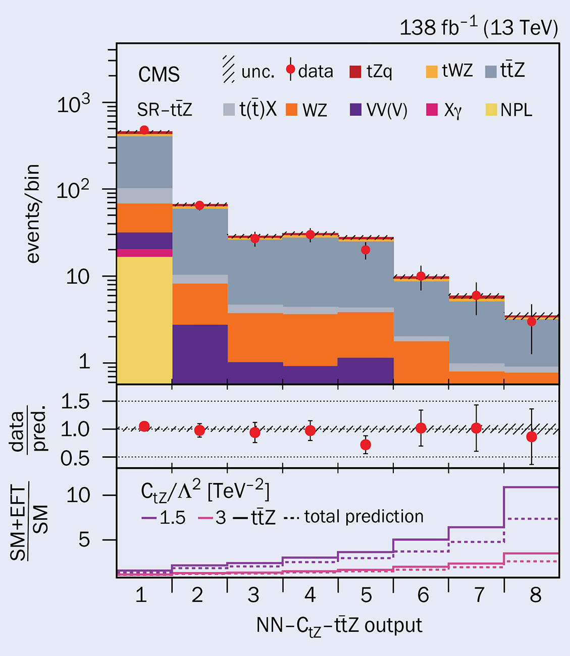


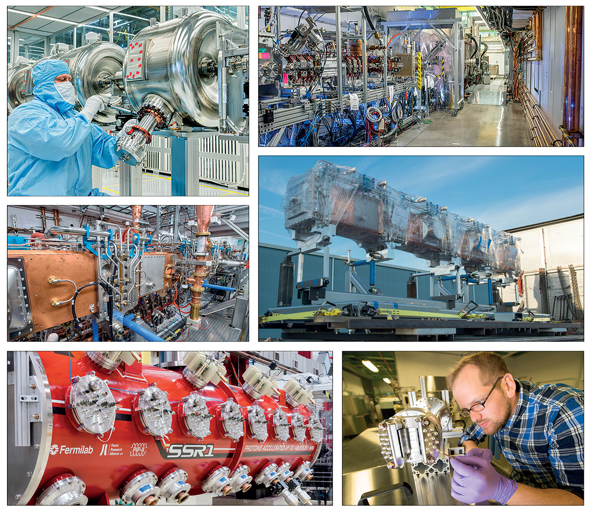
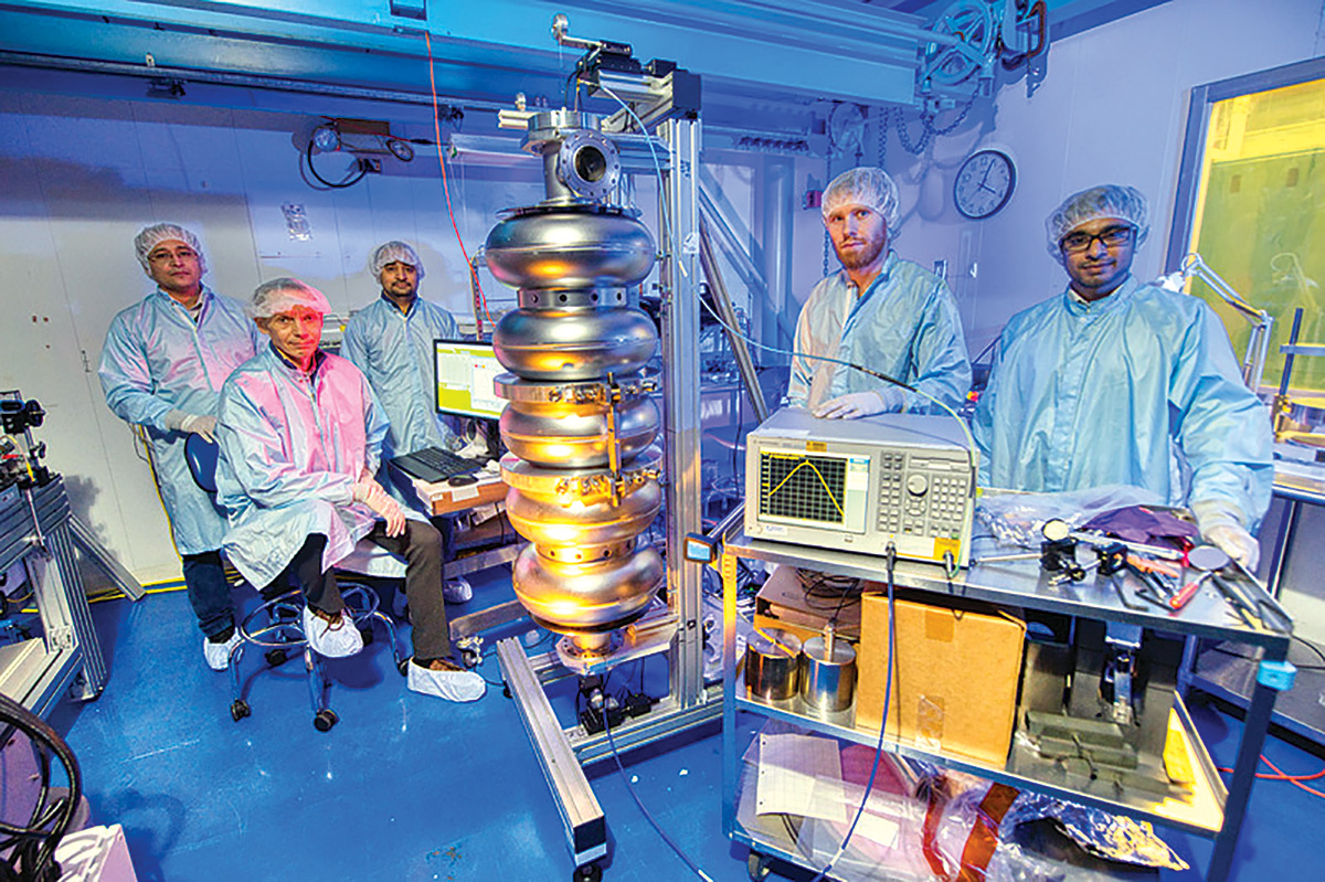
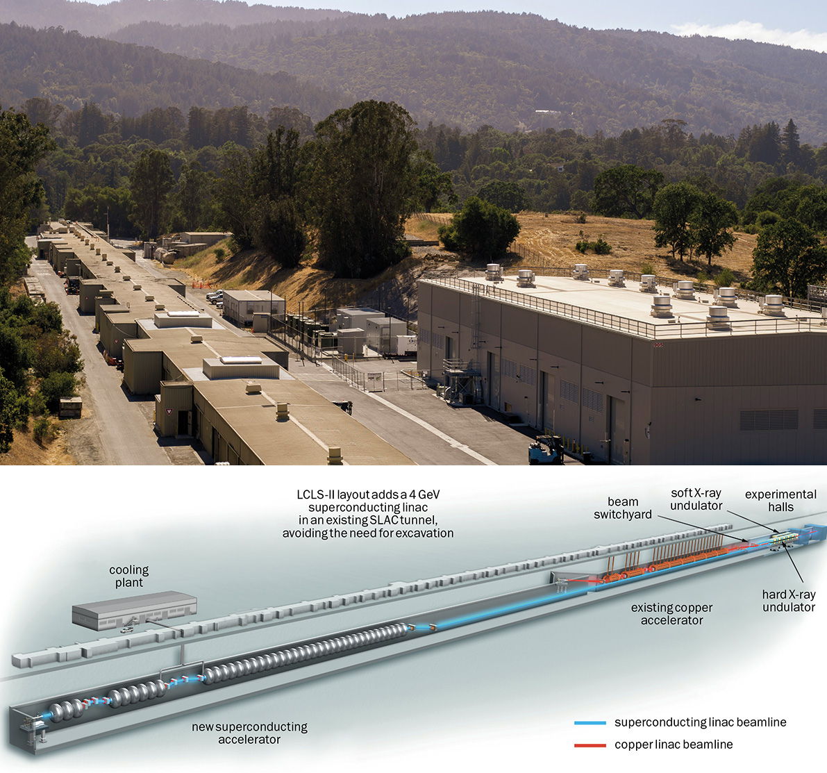

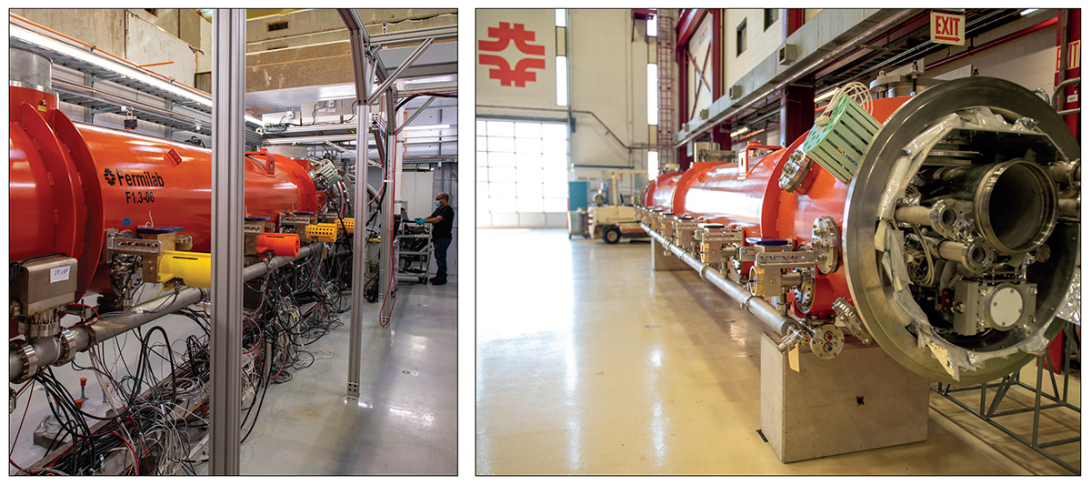
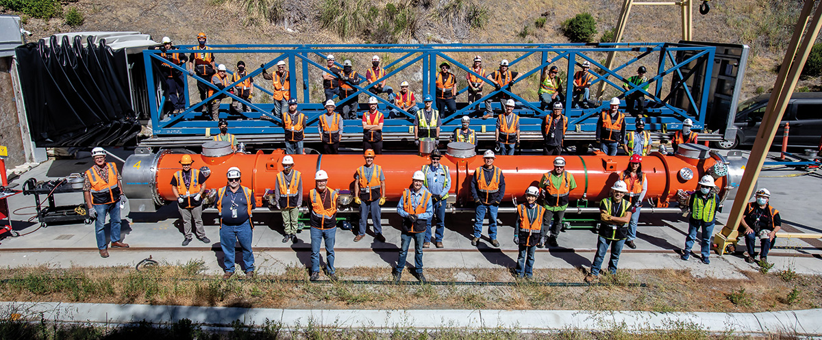
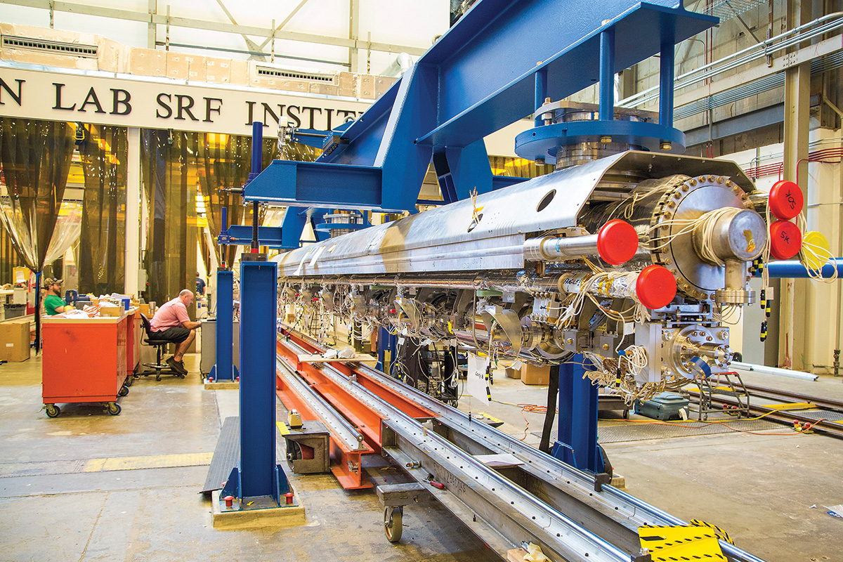

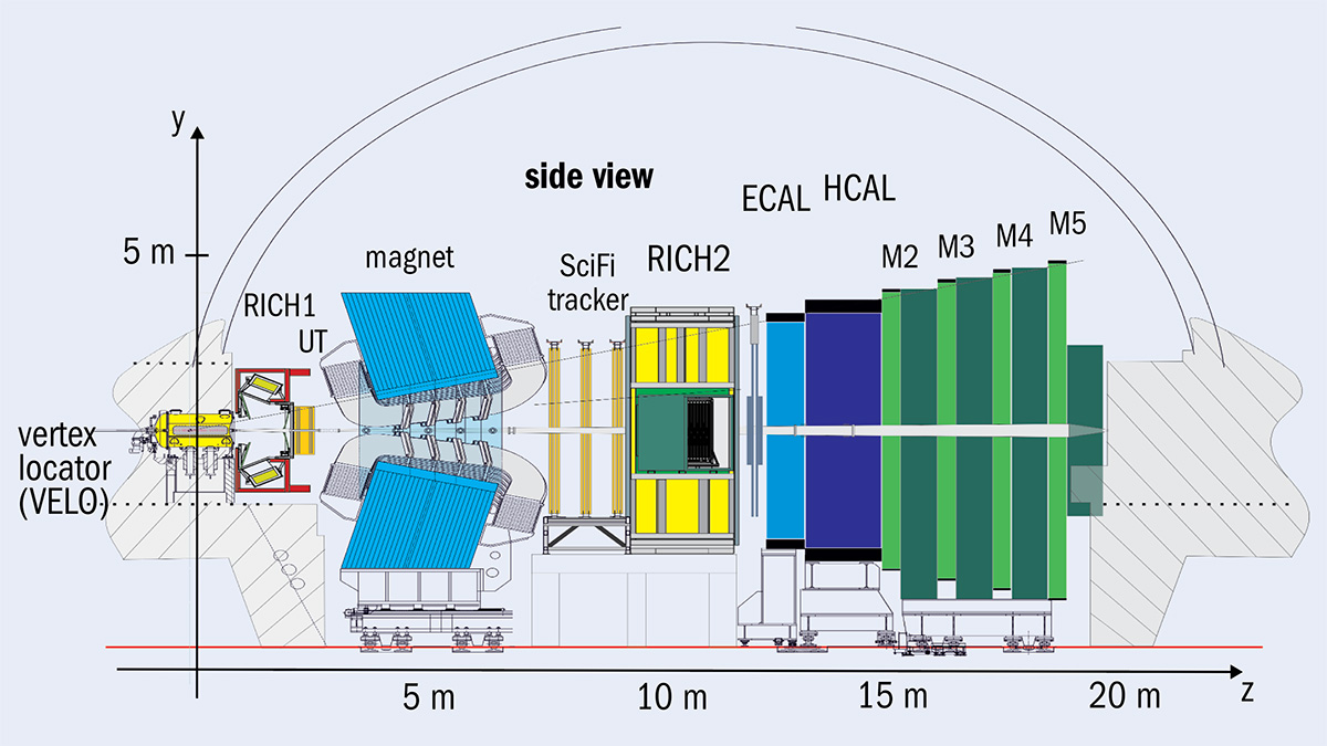
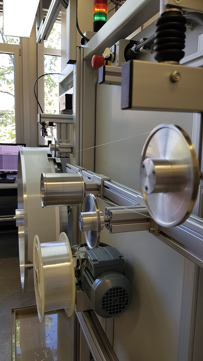
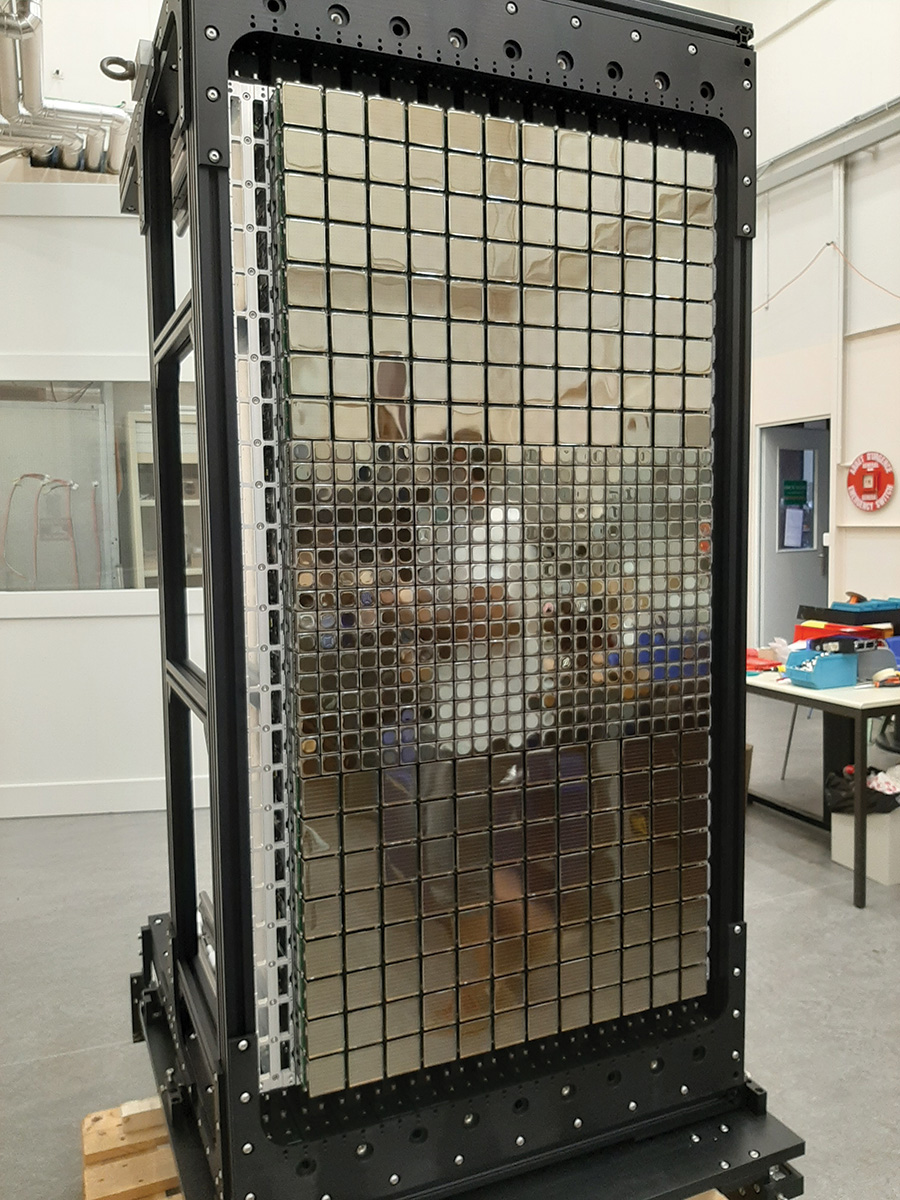
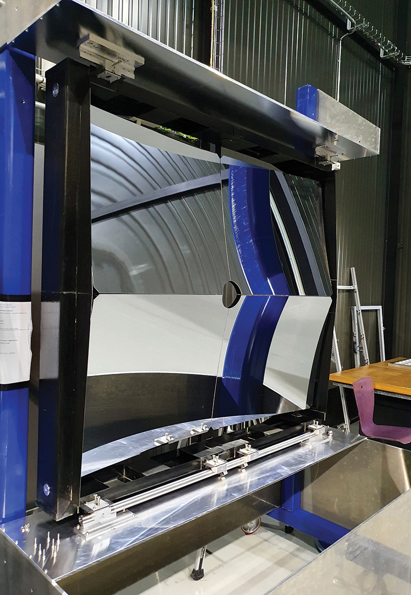


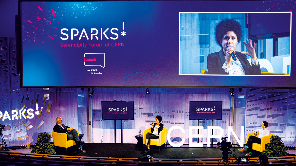


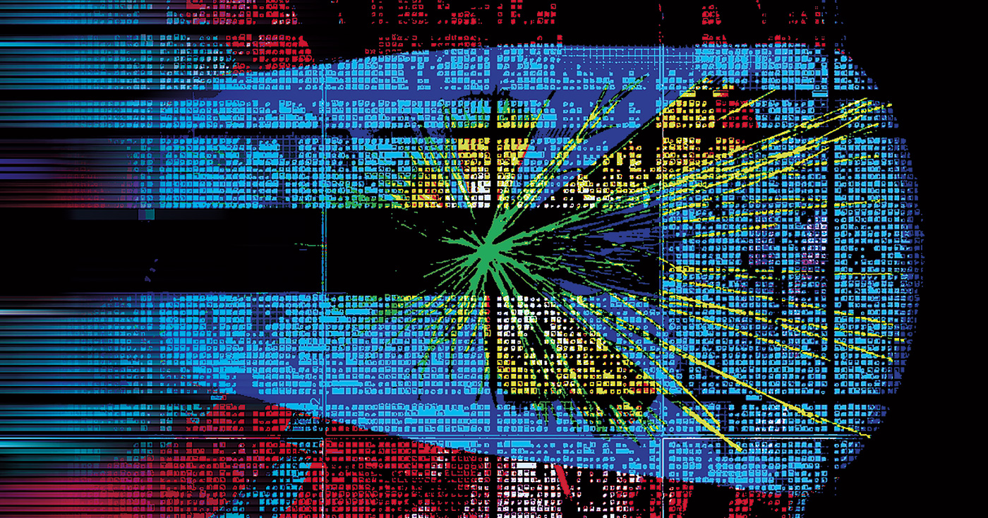

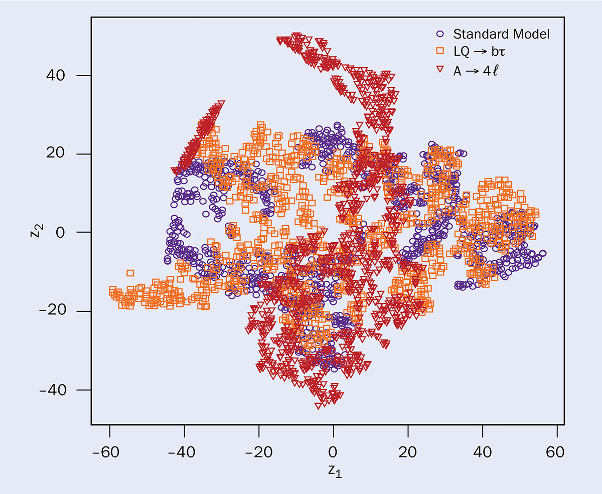
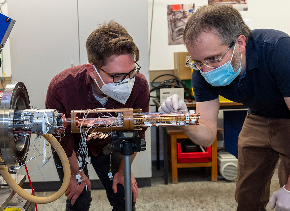
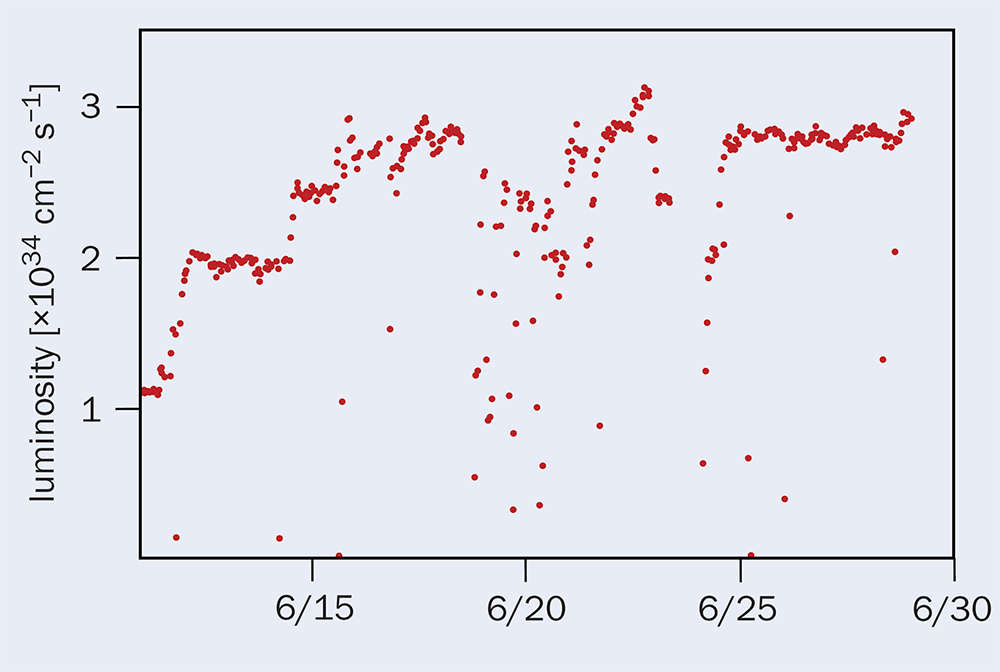
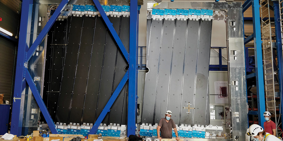