The conditions at CERN’s Large Hadron Collider pose severe challenges for the designers and builders of front-end, trigger and data acquisition electronics. A recent workshop reviewed the encouraging progress so far and discussed what remains to be done.
A decade ago, many aspects of the preparations for the major physics experiments for CERN’s Large Hadron Collider (LHC; scheduled to come into operation in 2005) appeared to be problematic. Particularly so were the front-end data acqusition electronics, which needed to be resistant to continual bombardment by high-energy collision products, and the trigger, which has to sift through the collisions for interesting results and reduce the original collision rate by a factor of about 10 million.
Fully aware that these preparations had to anticipate and take optimum advantage of rapid developments in modern microelectronics, a systematic research and development programme led by CERN’s Detector Research and Development Committee started to address these challenges and pave the road towards the LHC experiment proposals. However, the real work started once the projects had been approved. Progress has been marked by successive workshops of the Electronics Board of the LHC Experiments Committee. The most recent of these – the sixth in the series – was held in Cracow, Poland, in September 2000. The previous workshop was held in Snowmass, Colorado, and the workshop for 2001 is scheduled to take place in Stockholm, Sweden.
New challenges
At the time of the first of such workshops (1995-1997), designers were concentrating on individual designs, studying the basics of radiation effects and learning how to work with industry. Custom integrated circuit technology offered them the possibility of placing data buffering and first-level trigger filtering functions directly onto the detectors.
However, the process of developing mature integrated circuits turned out to be more time-consuming than had been anticipated. Testing was a bottleneck (one full design cycle takes about a year to complete), and using the special industrial technologies required to resist the LHC radiation environment involved a number of unexpected complications.
Meanwhile, the LHC community had realized that the experimental caverns would also present risks for the electronics, which needed to be, at the very least, “radiation tolerant”. Making sure that the many commercial off the-shelf components that were envisaged for the caverns were sufficiently radiation tolerant was a complex and difficult task.
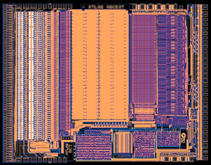
All of these challenges led the electronics development teams to search for new solutions, working hand-in-hand with other research labs and with industry. Today we have several designs ready, or almost ready, for production. A good example is the ABCD3T silicon tracker front-end chip for the giant ATLAS detector (figure 1).
This implements a binary read-out architecture in a 0.8 µm BiCMOS silicon-on-insulator technology, specially developed to meet the challenges of the LHC environment. Its equivalent for the big Compact Muon Solenoid (CMS) experiment – APV25 – reads out the data in analogue form and is implemented in a commercial 0.25 µm CMOS technology using a radiation-tolerant design technique developed for LHC. Both function according to the target design specifications.
Viable solutions
In addition, complex radiation-hard chips for the read-out of pixel detectors of all LHC experiments have now started to appear, a good example being the pixel read-out chip developed for the ALICE and LHCb experiments. This contains more than 13 million transistors and can be configured for tracking applications in ALICE or for particle identification in LHCb’s hybrid Ring Imaging Cerenkov detectors.
Prototype read-out boards for calorimeters and muon chambers have been shown to meet the functionality and performance specifications needed. However, not all of the components are sufficiently resistant to radiation yet, and further work is needed to optimize this aspect of the designs before launching production.
New problems, which are known as “single event upsets”, appeared as side-effects of the evolution of microelectronics technologies towards smaller feature sizes. Smaller charges are more easily perturbed, which often requires modifications to the design (e.g. selecting a more robust component, or using error detection/correction techniques).
For the optical read-out links, 1310 nm edge-emitting lasers have been selected for the analogue read-out of the CMS tracker, while 850 nm vertical cavity surface-emitting lasers appear to be a good choice for digital read-out links. Altogether it appears that viable solutions for the front-end detector electronics and optical read-out links have been found.
However, it will not be easy to integrate all of these components into the compact LHC detectors. Recent LHC Electronics Board (LEB) workshops tried to underline the system aspects of the LHC electronic designs: power supplies and distribution; grounding and shielding; cooling; timing and synchronization; and controls. The development groups are gradually attacking these issues and presenting solutions.
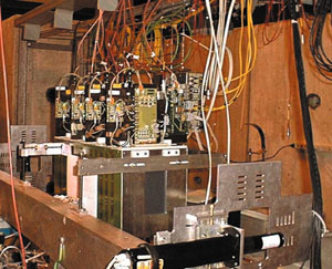
Figure 2 shows a small test set-up using prototypes of almost all of the elements foreseen for the read-out of the CMS tracker. To study issues such as timing and synchronization, it is being operated in a CERN test beam with a 25 ns structure, mimicking the 40 MHz LHC bunch-crossing frequency.
Nevertheless, large prototype system tests still have to be built and operated to prove that everything is understood and under control. This will require the mastery of complex test and assembly processes using state of-the-art technologies, for which available staffing is not always sufficient.
Close partnerships with industry and the adoption of common solutions (for crates, power supplies, cables, controls, etc) wherever possible will help to alleviate this problem. Other difficult issues include the maintenance and obsolesence of technologies over the relatively long timescale of the LHC project – already the very rapid pace of microelectronics advances has forced redesigns of several developments using new technology.
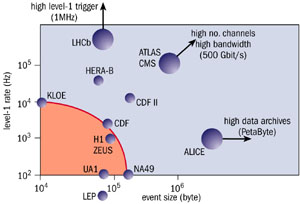
Triggering and data acquisition make up one of the extraordinary challenges facing detector designers at the high-luminosity LHC (figure 3). The LHCb trigger and data acquisition system must be able to handle trigger rates approaching 1 MHz, while the ALICE experiment operating in ion-ion collision mode must be able to handle large event sizes.
In the case of ATLAS and CMS, when LHC operates in proton collision mode at its nominal design luminosity of 1034 cm-2s-1, an average of 25 events are expected to occur at each bunch crossing, while bunch crossings will occur at a rate of 40 MHz. This input rate of 109 interactions every second must be reduced by a factor of at least 107 to about 100 Hz – the maximum rate that can be archived by the on-line computer farm.