The start of the LAA project in 1986 propelled electronics at CERN into a new era.
When the project for the Large Electron–Positron (LEP) collider began at CERN in the early 1980s, the programme required the concentration of all available CERN resources, forcing the closure not only of the Intersecting Storage Rings and its experiments, but of all the bubble chambers and several other fixed-target programmes. During this period, the LAA detector R&D project was approved at the CERN Council meeting in December 1986 as “another CERN programme of activities” (see box) opening a door to initiate developments for the future. A particular achievement of the project was to act as an incubator for the development of microelectronics at CERN, together with the design of silicon-strip and pixel detectors – all of which would become essential ingredients for the superb performance of the experiments at the LHC more than two decades later.
The start of the LAA project led directly to the build-up of know-how within CERN’s Experimental Physics Facilities Division, with the recruitment of young and creative electronic engineers. It also enabled the financing of hardware and software tools, as well as the training required to prepare for the future. By 1988, an electronics design group had been set up at CERN, dedicated to the silicon technology that now underlies many of the high-performing detectors at the LHC and in other experiments. Miniaturization to submicrometre scales allowed many functions to be compacted into a small volume in sophisticated, application-specific integrated circuits (ASICS), generally based on complementary metal-oxide-silicon (CMOS) technology. The resulting microchips incorporate analogue or digital memories, so selective read-out of only potentially useful data can be used to reduce the volume of data that is transmitted and analysed. This allows the recording of particle-collision events at unprecedented rates – the LHC experiments register 40 million events per second, continuously.
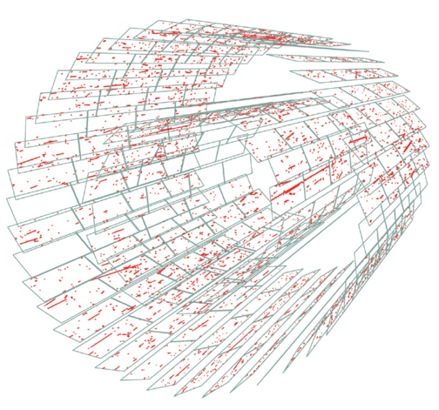
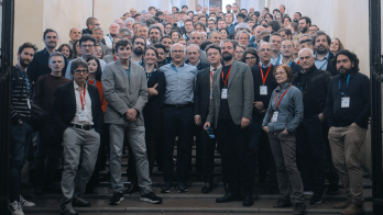
Last November, 25 years after the chip-design group was set up, some of those involved in the early days of these developments – including Antonino Zichichi, the initiator of LAA – met at CERN to celebrate the project and its vital role in establishing microelectronics at CERN. There were presentations from Erik Heijne and Alessandro Marchioro, who were among the founding members of the group, and from Jim Virdee, who is one of the founding fathers of the CMS experiment at the LHC. Together, they recalled the birth and gradual growth to maturity of microelectronics at CERN.
The beginnings
The story of advanced ASIC design at CERN began around the time of UA1 and UA2, when the Super Proton Synchrotron was operating as a proton–antiproton collider, to supply enough interaction energy for discovery of the W and Z bosons. In 1988, UA2 became, by chance, the first collider experiment to exploit a silicon detector with ASIC read-out. Outer and inner silicon-detector arrays were inserted into the experiment to solve the difficulty of identifying the single electron that comes from a decay of the W boson, close to the primary interaction vertex. The inner silicon-detector array with small pads could be fitted in the 9 mm space around the beam pipe, thanks to the use of the AMPLEX – a fully fledged, 16-channel 3-μm CMOS chip for read-out and signal multiplexing.
The need for such read-out chips was triggered by the introduction of silicon microstrip detectors at CERN in 1980 by Erik Heijne and Pierre Jarron. These highly segmented silicon sensors allow micrometre precision, but the large numbers of parallel sensor elements have to be dealt with by integrated on-chip signal processing. To develop ideas for such detector read-out, in the years 1984–1985 Heijne was seconded to the University of Leuven, where the microelectronics research facility had just become the Interuniversity MicroElectronics Centre (IMEC). It soon became apparent that CMOS technology was the way ahead, and the experience with IMEC led to Jarron’s design of the AMPLEX.
(Earlier, in 1983, a collaboration between SLAC, Stanford University Integrated Circuits Laboratory, the University of Hawaii and Bernard Hyams from CERN had already initiated the design of the “Microplex” – a silicon-microstrip detector read-out chip using nMOS, which was eventually used in the MARK II experiment at SLAC in the summer of 1990. The design was done in Stanford by Sherwood Parker and Terry Walker. A newer iteration of the Microplex design was used in autumn 1989 for the microvertex detector in the DELPHI experiment at LEP.)
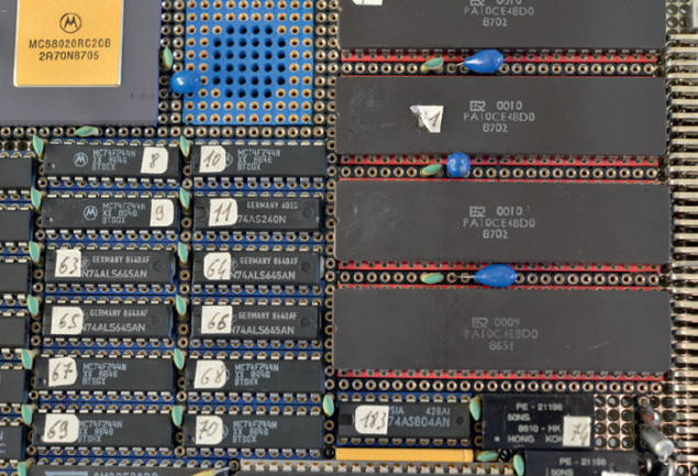
Heijne and Jarron were keen to launch chip design at CERN, as was Alessandro Marchioro, who was interested in developing digital microelectronics. However, finances were tight after the approval of LEP. With the appearance of new designs, the tools and methodologies developed in industry had to be adopted. For example, performing simulations was better than the old “try-and-test technique” of wire wrapping, but this required the appropriate software, including licences and training. The LAA project came at just the right time, allowing the chip-design group to start work in the autumn of 1988, with a budget for workstations, design software and analysis equipment – and crucially, up to five positions for chip-design engineers, most of whom remain at CERN to this day.
On the analogue side, there were three lines to the proposed research programme within LAA: silicon-microstrip read-out, a silicon micropattern pixel detector and R&D on chip radiation-hardness. The design of the first silicon-strip read-out chip at CERN – dubbed HARP for Hierarchical Analog Readout Processor – moved ahead quickly. The first four-channel prototypes were already received in 1988, with work such as the final design verification and layout check still being done at IMEC.
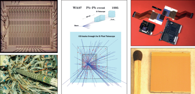
The silicon micropattern pixel detector, with small pixels in a 2D matrix, required integration of the sensor matrix and the CMOS read-out chip, either in the same silicon structure (monolithic) or in a hybrid technology with the read-out chip “bump bonded” to each pixel. Such a chip was developed as a prototype at CERN in 1989 in collaboration with Eric Vittoz of the Centre Suisse d’Electronique et de Microtechnique and his colleagues at the École polytechnique fédérale de Lausanne. While it turned out that this first chip could not be bump bonded, it successfully demonstrated the concept. In 1991, the next pixel-read-out chip designed at CERN was used in a three-unit “telescope” to register tracks behind the WA94 heavy-ion experiment in the Omega spectrometer. This test convinced the physicists to propose an improved heavy-ion experiment, WA97, with a larger telescope of seven double planes of pixel detectors. This experiment not only took useful data, but also proved that the new hybrid pixel detectors could be built and exploited.
Research on radiation hardness in chips remained limited within the LAA project, but took off later with the programme of the Detector Research and Development Committee (DRDC) and the design of detectors for the LHC experiments. Initially, it was more urgent to show the implementation of functioning chips in real experiments. Here, the use of AMPLEX in UA2 and later the first pixel chips in WA97 were crucial in convincing the community.
In parallel, components such as time-to-digital converters (TDCs) and other Fastbus digital-interface chips were successfully developed at CERN by the digital team. The new simulation tools purchased through the financial injection from the LAA project were used for modelling real-time event processing in a Fastbus data-acquisition system. This was to lead to high-performance programmable Fastbus ASICs for data acquisition in the early 1990s. Furthermore, a fast digital 8-bit adder-multiplier with a micropipelined architecture for correcting pedestals, based on a 1.2 μm CMOS technology, was designed and used in early 1987. By 1994, the team had designed a 16-channel TDC for the NA48 experiment, with a resolution of 1.56 ns, which could be read out at 40 MHz. The LAA had well and truly propelled the engineers at CERN into the world of microtechnology.
The LAA
The LAA programme, proposed by Antonino Zichichi and financed by the Italian government, was launched as a comprehensive R&D project to study new experimental techniques for the next step in hadron-collider physics at multi-tera-electron-volt energies. The project provided a unique opportunity for Europe to take a leading role in advanced technology for high-energy physics. It was open to all physicists and engineers interested in participating. A total of 40 physicists, engineers and technicians were recruited, and more than 80 associates joined the programme. Later in the 1990s, during the operation of LEP for physics, the programme was complemented by the activities overseen by CERN’s Detector R&D Committee.
The challenge for the LHC
A critical requirement for modern high-energy-physics detectors is to have highly “transparent” detectors, maximizing the interaction of particles with the active part of the sensors while minimizing similar interactions with auxiliary material such as electronics components, cables, cooling and mechanical infrastructure – all while consuming absolute minimum power. Detectors with millions of channels can be built only if each channel consumes milliwatts of power. In this context, the developments in microelectronics offered a unique opportunity, allowing the read-out system of each detector to be designed to provide optimal signal-to-noise characteristics for minimal power consumption. In addition, auxiliary electronics such as high-speed links and monitoring electronics could be highly optimized to provide the best solution for system builders.
However, none of this was evident when thoughts turned to experiments for the LHC. The first workshop on the prospects for building a large proton collider in the LEP tunnel took place in Lausanne in 1984, the year following the discovery of the W and Z bosons by UA1 and UA2. A prevalent saying at the time was “We think we know how to build a high-energy, high-luminosity hadron collider – we don’t have the technology to build a detector for it.” Over the next six years, several seminal workshops and conferences took place, during the course of which the formidable experimental challenges started to appear manageable, provided that enough R&D work could be carried out, especially on detectors.
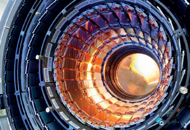
The LHC experiments needed special chips with a rate capability compatible with the collider’s 40 MHz/25 ns cycle time and with a fast signal rise time to allow each event to be uniquely identified. (Recall that LEP ran with a 22 μs cycle time.) Thin – typically 0.3 mm – silicon sensors could meet these requirements, having a dead time of less than 15 ns. With sub-micron CMOS technology, front-end amplifiers could also be designed with a recovery time of less than 50 ns, therefore avoiding pile-up problems.
Thanks to the LAA initiative and the launch in 1990 by CERN of R&D for LHC detectors, overseen by the DRDC, technologies were identified and prototyped that could operate well in the harsh conditions of the LHC. In particular, members of the CERN microelectronics group pioneered the use of special full custom-design techniques, which led to the production of chips capable of withstanding the extreme radiation environment of the experiments while using a commercially available CMOS process. The first full-scale chip developed using these techniques is the main building block of the silicon-pixel detector in the ALICE experiment. Furthermore, in the case of CMS, the move to sub-micron 0.25-μm CMOS high-volume commercial technology for producing radiation-hard chips enabled the front-end read-out for the tracker to be both affordable and delivered on time. This technology became the workhorse for the LHC and has been used since for many applications, even where radiation tolerance is not required.
An example of another area that benefited from an early launch, assisted by the LAA project, is optical links. These play a crucial role in transferring large volumes of data, an important example being the transfer from the front ends of detectors that require one end of the link to be radiation hard – again, a new challenge.
Today, applications that require a high number of chips can profit from the increase in wafer size, with many chips per wafer, and low cost in high-volume manufacturing. This high level of integration also opens new perspectives for more complexity and intelligence in detectors, allowing new modes of imaging.
Looking ahead
Many years after Moore’s law was suggested, miniaturization still seems to comply with it. There has been continuous progress in silicon technology, from 10 μm silicon MOS transistors in the 1970s to 20 nm planar silicon-on-insulator transistors today. Extremely complex FinFET devices promise further downscaling to 7 nm transistors. Such devices will allow even more intelligence in detectors. The old dream of having detectors that directly provide physics primitives – namely, essential primary information about the phenomena involved in the interaction of particles with matter – instead of meaningless “ADC counts” or “hits” is now fully within reach. It will no longer be necessary to wait for data to come out of a detector because new technology for chips and high-density interconnections will make it possible to build in direct vertex-identification, particle-momenta evaluation, energy sums and discrimination, and fast particle-flow determination.
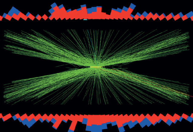
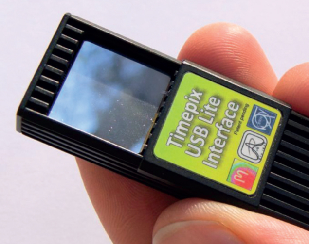
Some of the chips developed at CERN – or the underlying ideas – have found applications in materials analysis, medical imaging and various types of industrial equipment that employ radiation. Here, system integration has been key to new functionalities, as well as to cost reduction. The Medipix photon-counting chip developed in 1997 with collaborators in Germany, Italy and the UK is the ancestor of the Timepix chip that is used today, for example, for dosimetry on the International Space Station and in education projects. Pixel-matrix-based radiation imaging also has many applications, such as for X-ray diffraction. Furthermore, some of the techniques that were pioneered and developed at CERN for manufacturing chips sufficiently robust to survive the harsh LHC conditions are now adopted universally in many other fields with similar environments.
Looking ahead to Europe’s top priority for particle physics, exploitation of the LHC’s full potential until 2035 – including the luminosity upgrade – will require not only the maintenance of detector performance but also its steady improvement. This will again require a focused R&D programme, especially in microelectronics because more intelligence can now be incorporated into the front end.
Lessons learnt from the past can be useful guides for the future. The LAA project propelled the CERN electronics group into the new world of microelectronic technology. In the future, a version of the LAA could be envisaged for launching CERN into yet another generation of discovery-enabling detectors exploiting these technologies for new physics and new science.


