Different technologies come together in the gas pixel detector, a device that for the first time brings very high resolving power to gas detectors, as Ronaldo Bellazzini explains.
Over the past decade micropattern gas detectors (MPGDs) have become increasingly important, not only in high-energy physics but also in other applications where high spatial resolution is required together with operation at high rates. MPGDs are position-sensitive proportional counters, descendents of the multiwire chambers that amplify and collect charge released as ionizing particles pass through a volume of gas. The difference with MPGDs is that the electrodes that sense the avalanche of charge are constructed using microelectronics, thin-film or advanced printed circuit board (PCB) techniques. With such methods, feature sizes of just a few microns can be achieved, leading to detectors that have excellent spatial resolution and fast charge collection.
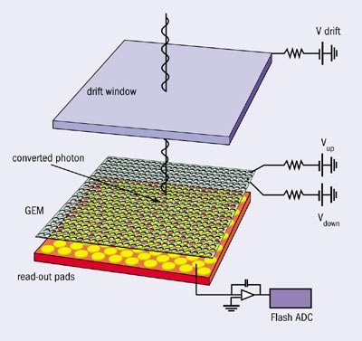
One attractive class of MPGD is the gas electron multiplier (GEM) detector, which can fully decouple the charge-amplification structure from the read-out structure. The GEM concept uses a thin sheet of metalized plastic pierced by a regular array of tiny, closely spaced holes. When a voltage is applied across the device, the high electric field at the holes causes an avalanche of charge, which can be collected by a read-out electrode. In this way, the charge amplification and read-out can be independently optimized. For example, by organizing the read-out plane in a multipixel pattern it is possible to obtain true 2D imaging capability (see figure 1). The high granularity of the pixelated read-out plane preserves the intrinsic resolving power of the device and its high rate capability, which are otherwise unavoidably lost if a conventional projective read-out approach is used – for example, with a read-out on x and y axes (Bellazzini and Spandre 2003).
However, when the pixel size is small (less than 100 µm) and the number of pixels is large (more than 1000), it is virtually impossible to bring the signal charge from individual pixels in the GEM read-out to a chain of external read-out electronics, even if advanced, fine-line, multilayer PCB technology is used. The fan-out connecting the segmented anodes that collect the charge to the front-end electronics is the real bottleneck: technological constraints limit the number of independent electronics channels that can be brought to the peripheral electronics. Furthermore, the cross-talk between adjacent channels and the noise that is caused by the high-input capacitance to the pre-amplifiers become significant.

The solution is that, rather than take the signal from the pixel to the read-out electronics, the electronics chain has to be brought to the individual pixel. This concept has been developed recently at INFN Pisa, where deep, submicron VLSI technology was used to build an application-specific integrated circuit (ASIC) to perform both charge collection and read-out. The top metal layer of the ASIC consists of a CMOS array of 2101 active pixels with an 80 µm pitch, which is used directly as the charge-collecting anode of a GEM. Each charge-collecting pad of the array is connected to a full electronics chain (pre-amplifier, shaping amplifier, sample-and-hold, multiplexer) built immediately below the pad using the five remaining active layers of the VLSI structure. With this approach, gas detectors have for the first time reached the level of integration and resolution typical of solid-state pixel detectors (Bellazzini et al. 2004).
The ASIC was created using 0.35 µm, 3.3 V CMOS technology. Figure 2 shows the device layout as seen from the top metal layer. The active matrix, in pink, is surrounded by a passive guard ring of 3-4 pixels, which are set to the same potential as the active pixels. Figure 3 shows the actual chip bonded to its ceramic package.

To build the complete detector, a single GEM MPGD with an active gas volume of less than 1 cm3 is assembled directly over the chip containing the ASIC, which forms both the charge-collecting anode and the pixelized read-out of the MPGD, so that the detector and the read-out electronics become a single unit. This enables the full electronics chain and the detector to be completely integrated without the need for complicated bump bonding.
In the prototype there is a drift region (absorption gap) of 6 mm above the GEM foil, while a 1 mm spacer defines the collection gap between the lower surface of the GEM and the pixel matrix of the read-out chip. The GEM has a standard thickness of 50 µm and holes of 50 µm diameter at 90 µm pitch on a triangular pattern. The entrance window is made from 25 µm thick Mylar foil, aluminized on one side. Typical applied voltages are 1000 V (drift electrode), -500 V (top of GEM) and -100 V (bottom of GEM) – the collecting electrodes being around 0 V. In these conditions the detector operates at a typical gain of 1000.
Thanks to the very low pixel capacitance at the preamplifier input, a noise level of 1.8 mV was measured, which corresponds to around 100 electrons. This means that with the gas gain of 1000, the detector has significant sensitivity to a single primary electron.
The first application of this new MPGD concept is for an X-ray polarimeter, for use in astronomy, operating in the low-energy band (1-10 keV). Information on the degree and angle of polarization of astronomical sources can be derived from the angular distribution of the initial part of the photoelectron tracks when they are projected onto a finely segmented 2D imaging detector.

The algorithm for the reconstruction of the photoelectron path begins with the evaluation of the first moment (M1) of the charge distribution on the read-out pixels, and the maximization of the second moment (M2) of the charge distribution to define the principal axis of the track. In a further step, the asymmetry of the charge release along the principal axis (third moment, M3) is computed and the conversion point is derived by moving along this axis in the direction of negative M3, where the released charge is smaller by a length of around M2. The reconstruction of the direction of emission is then carried out by taking into account only the pixels in a region weighted according to the distance from the estimated conversion point.
The morphology of a real track obtained by illuminating the device with a low-energy radioactive source (5.9 keV X-ray from 55Fe) is shown in figure 4. The small cluster owing to the Auger electron and the initial part of the track can be distinguished from the larger Bragg peak. The plot of the raw signals of all of the channels for the same event shows the optimal signal-to-noise ratio obtained using this detector (figure 5). Around 50,000 electrons from the gas-amplified primary photoelectrons are divided between 53 pixels.

The final design for our X-ray polarimeter application (Costa et al. 2001) will have 16-32 K channels with a pixel size of 60-70 µm and an active area of around 1 cm2. However, many other applications can be foreseen, depending on various factors, such as the size of the pixels and the die, the electronics shaping time, the analogue versus digital read-out, counting versus integrating mode and gas filling. Such developments would surely open new directions in gas proportional detectors, and bring the field to the same level of integration as that of solid-state detectors.
Further reading
R Bellazzini and G Spandre 2003 Nuclear Instruments and Methods in Physics Research A 513 231.
R Bellazzini et al. 2004.
E Costa et al. 2001 Nature 411 662.