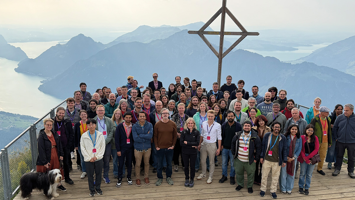
The 34th International Workshop on Vertex Detectors, VERTEX 2026, was held from 20 to 24 July in Stoos, a car-free village in the canton of Schwyz. Organised by the University of Zurich, the Paul Scherrer Institute and ETH Zurich, it brought together about 100 participants. Since 1992, the series has followed the development of semiconductor-based vertex and tracking detectors for particle physics, together with the applications they find beyond the field.
Lake reflections
In 2001, the 10th edition of the workshop took place in Brunnen, on Lake Lucerne, almost 900 metres below Stoos. The return invites reflection on what the community expected then, what it has since achieved and what the coming 25 years may ask of it, with an electron–positron Future Circular Collider (FCC-ee) newly recommended as the preferred option for CERN’s next flagship collider.
A quarter of a century ago, the hybrid architecture – in which sensor and readout chip are fabricated separately and then bonded together – was regarded as the only one able to combine the readout speed, radiation tolerance and spatial resolution demanded by the LHC. At Stoos, the vertex and tracking detectors of ATLAS, CMS and LHCb, presented respectively by Martin Kocian (SLAC), Davide Zuolo (University of Colorado Boulder) and David Vico Benet (University of Oxford), were again all hybrids, as are the successor systems now being built for the High-Luminosity LHC. Both halves of the assembly have moved on. Double-sided n-in-n planar sensors have given way to single-sided n-in-p designs, and to 3D sensors in the innermost layers, while readout chips have followed the industry down to smaller CMOS nodes, more tolerant of radiation and small enough to put finer pixels and more logic behind each one.
Much of the programme was given over to low-gain avalanche detectors
The community of 2001 was concerned with position measurement and with sensors able to survive the LHC’s expected fluences. These concerns remain, but at Stoos a third stood beside them: timing. Much of the programme was given over to low-gain avalanche detectors (LGADs), in which a thin, highly doped gain layer multiplies the signal enough to be timed to a few tens of picoseconds.
The gain layer is difficult to segment finely while keeping a uniform spatial response, and several LGAD variants address the problem. Some leave it unsegmented and reconstruct the hit position from the charge shared between neighbouring electrodes, by resistive or capacitive coupling, as presented by Roberta Arcidiacono (University and INFN Torino) and Koji Nakamura (KEK). Others, discussed by Anna Macchiolo (University of Zurich), use trench isolation to minimise the no-gain region between electrodes. The unsegmented designs promise space and time resolution at once, at a lower power density, because their coarser pitch more than compensates for a higher consumption per channel. Whether that balance survives contact with a full-size detector is one of the questions of the coming years.
Making gains
A second problem comes from the gain layer itself, which irradiation progressively deactivates as radiation-induced defects trap the acceptors, the dopant atoms that create the strong electric field responsible for the gain. Answers at Stoos ranged from co-doping the gain implant with carbon, which slows this loss, to compensated designs, presented by Valentina Sola (University and INFN Torino). In these, a matching loss of co-implanted donors, dopants of the opposite type, offsets the loss of acceptors. Micromachined devices dispense with the doped layer altogether and create the gain through the shape of their electrodes, while internal multiplication in wide-bandgap semiconductors such as silicon carbide is also being explored.
Timing is not the sensor’s work alone. For 4D tracking, which measures position and time together, a time stamp of a few tens of picoseconds must be produced within each pixel. The move to a 28 nm CMOS process, a chip technology with smaller transistors, makes room in every cell for the circuitry this requires, from the converter that turns a signal’s arrival into a digital time to the distribution of a stable reference clock.
The interconnection itself has barely changed since 2001. Fine-pitch bump bonding, in which tiny solder bumps join each sensor chip to its readout chip one pair at a time, equips every LHC and High-Luminosity LHC pixel detector. But it remains largely manual and needs full sensor and readout wafers as input, which caps throughput and makes prototyping expensive. Fabian Hügging (University of Bonn) presented two routes out. For prototypes and small volumes, the process is moving in house, using anisotropic conductive films and pastes, in which conductive particles held in an insulating adhesive link each pair of facing pads when pressed together. For performance and throughput, the route is to bond whole sensor and readout wafers, using through-silicon vias – vertical connections etched through the thinned readout chip – to carry the signals out from its back. This would allow far thinner readout chips on far thinner sensors.
The forward-looking half of the programme was almost uniformly monolithic
In Brunnen, the monolithic sensor had been flagged as an architecture worth watching, and time has confirmed that judgement. Where radiation tolerance is not the constraint, material budget and power take over, and there, monolithic designs, in which readout electronics and sensor share the same silicon die and the interconnection step disappears, have taken the ground. Anna Villani (University and INFN Trieste) reported on the ALICE ITS2, the largest application of monolithic active pixel sensors yet built, and Kookhyun Kang (Kyungpook National University) on Belle II, which uses partially monolithic DEPFET sensors. Luigi Vigani (Heidelberg University) presented the Mu3e pixel tracker at PSI, the first tracker built from monolithic sensors on a high-voltage process.
The forward-looking half of the programme was almost uniformly monolithic. Monolithic sensors were presented as the prime candidates for the FCC-ee vertex detector by Armin Ilg (University of Zurich) and Gherardo Ammirabile (University and INFN Pisa), in layouts of thin, curved and overlapping devices whose power dissipation is low enough for air cooling, and CMOS sensors are included to equip several other future-experiment designs. One further step would close the circle. A shallow gain implant beneath the collection electrode turns a monolithic sensor into an LGAD, and should that succeed, a detector would no longer have to choose between ultra-low mass and precise timing.
Classifying clusters
A new arrival on the programme was machine learning inside detector front-ends. Faced with data volumes that outgrow what can be read out, several talks proposed moving the decision on what to keep closer to the sensor. A readout chip presented by Jennet Dickinson (Cornell University) places a neural network within the pixel array, classifying clusters before the data leave the chip, while Mathieu Benoit (Oak Ridge National Laboratory) explored neuromorphic networks whose spiking behaviour matches the event-driven output of the sensor. What is at stake is whether the innermost tracking layers, which measure the impact parameter best, can take part in the trigger decision at all.
Five days of open exchange, in a setting that keeps everyone together, send people home with ideas and perspectives they did not arrive with. That is reason enough to go up the mountain again.