The first upgrade of the pixel system in the ATLAS experiment will incorporate radiation-hard 3D silicon detectors designed by a team of physicists and engineers who worked in conjunction with processing laboratories to move rapidly from R&D to production.

Three-dimensional silicon sensors are opening a new era in radiation imaging and radiation-hard, precise particle-tracking through a revolutionary processing concept that brings the collecting electrodes close to the carriers generated by ionizing particles and that also extends the sensitive volume to a few microns from the physical sensor’s edge. Since the summer of 2011, devices as large as 4 cm2 with more than 100,000 cylindrical electrodes have become available commercially thanks to the vision and effort of a group of physicists and engineers in the 3DATLAS and ATLAS Insertable B-Layer (IBL) collaborations who worked together with the original inventors and several processing laboratories in Europe and the US. This unconventional approach enabled a rapid transition from the R&D phase to industrialization, and has opened the way to being able to use more than 200 such sensors in the first upgrade in 2014 of the pixel system in the ATLAS experiment.
Radiation effects
Silicon sensors with 3D design were proposed 18 years ago at the Stanford Nanofabrication Facility (SNF) to overcome the limitations of the poor signal-efficiency of gallium-arsenide sensors, a problem that affects silicon sensors after exposure to heavy non-ionizing radiation. The study of microscopic and macroscopic properties of irradiated silicon was, and still is, the subject of extensive studies in several R&D groups and has led to the identification of stable defects generated after exposure to neutral or charged particles. The presence of such defects makes the use of silicon as a detector challenging in the highly exposed inner trackers of high-energy-physics experiments. The studies have discovered that while some of these defects act as generation centres, others act as traps for the moving carriers generated by incident particles produced in the primary collisions of accelerator beams. The three most severe macroscopic consequences for silicon-tracking detectors that have been found concern linearly proportional increases in the leakage current and in the effective doping concentration with increasing fluence, as well as severe signal loss that arises from trapping.
Apart from applications in high-energy physics, 3D sensor technology has potential uses in medical, biological and neutron imaging
However, other studies have found evidence that the spatial proximity of the p+ and n+ electrodes in the pin junction not only allows it to be depleted with a reduced bias-voltage but also that the highest useful electric field across the junction can be applied homogeneously to reduce the trapping probability of generated carriers after radiation-induced defects are formed. This leads to less degradation of the signal efficiency – defined as the ratio of irradiated versus non-irradiated signal amplitudes – after exposure at increasing radiation fluences.
What now makes 3D radiation sensors one of the most radiation-hard designs is that the distance between the p+ and n+ electrodes can be tailored to match the best signal efficiency, the best signal amplitude and the best signal-to-noise or signal-to-threshold ratio to the expected non–ionizing radiation fluence. Figure 1 indicates how this is possible by comparing planar sensors – where electrodes are implanted on the top and bottom surfaces of the wafer – with 3D ones. The sketch on the left shows how the depletion region between the two electrodes, L, grows vertically to become as close as possible to the substrate thickness, Δ. This means that there is a direct geometrical correlation between the generated signal and the amplitude of the depleted volume. By contrast, in 3D sensors (figure 1, right) the electrode distance, L, and the substrate thickness, Δ, can be decoupled because the depletion region grows laterally between electrodes whose separation is a lot smaller than the substrate thickness. In this case, the full depletion voltage, which depends on L and grows with the increase of radiation-induced space charge, can be reduced dramatically.
For the same substrate thickness – before or at moderate irradiation – the amount of charge generated by a minimum-ionizing particle is the same for both types of sensor. However, because the charge-collection distance in 3D sensors is much shorter – and high electric fields as well as saturation of the carrier velocity can be achieved at low bias-voltage – the times for charge collection can be much faster. Apart from making applications that require high speeds easier, this property can counteract the charge–trapping effects expected at high radiation levels. A 3D sensor reaching full depletion at less than 10 V before irradiation can operate at just 20 V and provide full tracking efficiency. After the heavy irradiation expected for the increased LHC luminosity, the maximum operational bias-voltage can be limited to 200–300 V. This has a crucial impact on the complexity of the biasing and cooling systems needed to keep the read-out electronics well below the temperatures at which heat-induced failures occur. By comparison, the voltages required to extract a useful signal when L increases, for example in planar sensors, can be as high as 1000 V.
These 3D silicon sensors are currently manufactured on standard 4-inch float-zone-produced, p-type, high-resistivity wafers, using a combination of two well established industrial technologies: micro-electro-mechanical systems (MEMS) and very large scale integration (VLSI). VLSI is used in microelectronics and in the fabrication of traditional silicon microstrip and pixel trackers in high-energy-physics experiments, as well as in the CCDs used in astronomy and in many kinds of commercial cameras, including those in mobile phones. A unique aspect of the MEMS technology is the use of deep-reactive ion etching (DRIE) to form deep and narrow apertures within the silicon wafer using the so-called “Bosch process”, where etching is followed first by the deposition of a protective polymer layer and then by thermal-diffusion steps to drive in dopants to form the n+ and p+ electrodes.
Two methods
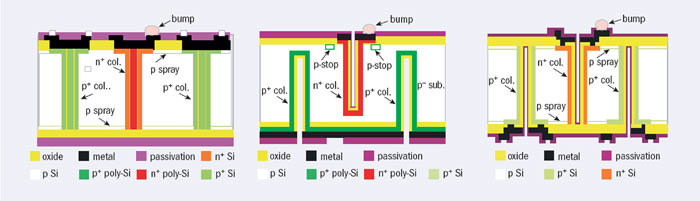
Currently, two main 3D-processing options exist. The first, called Full3D with active edges, is based on the original idea. It is fabricated at SNF at Stanford and is now also available at SINTEF in Oslo. In this option, column etching for both types of electrodes is performed all through the substrate from the front side of the sensor wafer. At the same time, active ohmic trenches are implemented at the edge to form so-called “active edges”, whereas the underside is oxide-bonded to a support wafer to preserve mechanical robustness. This requires extra steps to attach and remove the support wafer when the single sensors are connected to the read-out electronics chip. An additional feature of this approach is that the columns and trenches are completely filled with poly-silicon (figure 2, left).
The second approach, called double-side with slim fences is a double-side process, developed independently in slightly different versions by Centro Nacional de Microelectrónica (CNM) in Barcelona and Fondazione Bruno Kessler (FBK) in Trento. While in both cases junction columns are etched from the front side and ohmic columns from the back side, without the presence of a support wafer, in CNM sensors columns do not pass through the entire wafer thickness but stop a short distance from the surface of the opposite wafer-side (figure 2, centre). This was also the case for the first prototypes of FBK sensors but the technology was later modified to allow for the columns to pass through (figure 2, right).
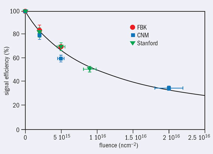
While all of the remaining processing steps after electrode etching and filling are identical for a 3D sensor to those of a planar silicon sensor – so that hybridization with front-end electronics chips and general sensor handling is the same – the overall processing time is longer, which limits the production-volume capability for a single manufacturer at a given time. For this reason, to speed up the transition from R&D to industrialization, the four 3D-silicon-processing facilities (SNF, SINTEF, CNM and FBK) agreed to combine their expertise for the production of the required volume of sensors for the first ATLAS upgrade, the IBL. Based on the test results obtained in 2007–2009, which demonstrated a comparable performance between different 3D sensors both before and after irradiation, the collaboration decided in June 2009 to go for a common design and joint processing effort, aiming at a full mechanical compatibility and equivalent functional performance of the 3D sensors while maintaining the specific flavours of the different technologies. Figure 3 demonstrates the success of this strategy by showing a compilation of signal efficiencies versus fluence (in neutron equivalent per square centimetre) of samples from different manufacturers after exposure to heavy irradiation. Their position fits the theoretical parameterization curve, within errors.
All of these 3D-processing techniques were successfully used to fabricate sensors compatible with the FE-I4 front-end electronics of the ATLAS IBL. FE-I4 is the largest front-end electronics chip ever designed and fabricated for pixel-vertex detectors in high-energy physics and covers an area of 2.2 × 1.8 cm2 with 26,880 pixels, each measuring 250 × 50 μm2. These will record images of the production of the primary vertex in proton–proton collisions, 3.2 cm from the LHC beam in the IBL. Each 3D sensor uses two n electrodes tied together by an aluminium strip to cover the 250 μm pixel length. This means that each sensor has more than 100,000 holes.
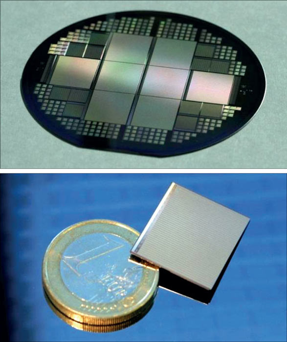
Currently more than 60 wafers of the kind shown in figure 4 made with double-sided processing – which do not require support-wafer removal and have 200 μm slim fences rather than active edges – are at the IZM laboratory in Berlin, where single sensors will be connected with front-end electronics chips using bump-bonding techniques to produce detector modules for the IBL. Each wafer hosts eight such sensors, 62% of which have the required quality to be used for the IBL.
What’s next?
Following the success of the collaborative effort of the 3DATLAS R&D project, the industrialization of active-edge 3D sensors with even higher radiation hardness and a lighter structure is the next goal in preparation for the LHC High-Luminosity Upgrade beyond 2020. Before that, 3D sensors will be used in the ATLAS Forward Physics project, where sensors will need to be placed as close to the beam as possible to detect diffractive protons at 220 m on either side of the interaction point. Apart from applications in high-energy physics, where microchannels can also be etched underneath integrated electronics substrates for cooling purposes, 3D sensor technology is used to etch through silicon vias (TSV) in vertical integration, to fabricate active edge with planar central electrodes and has potential use in medical, biological and neutron imaging. The well defined volume offered by the 3D geometry is also ideal for microdosimetry at cell level.